- 您现在的位置:买卖IC网 > PDF目录1829 > LTC3240EDC-2.5#TRPBF (Linear Technology)IC REG MULTI CONFIG 2.5V 6DFN PDF资料下载
参数资料
| 型号: | LTC3240EDC-2.5#TRPBF |
| 厂商: | Linear Technology |
| 文件页数: | 9/12页 |
| 文件大小: | 0K |
| 描述: | IC REG MULTI CONFIG 2.5V 6DFN |
| 标准包装: | 2,500 |
| 类型: | 降压(降压),升压(升压),切换电容(充电泵) |
| 输出类型: | 固定 |
| 输出数: | 1 |
| 输出电压: | 2.5V |
| 输入电压: | 1.8 V ~ 5.5 V |
| PWM 型: | Burst Mode? |
| 频率 - 开关: | 1.2MHz |
| 电流 - 输出: | 150mA |
| 同步整流器: | 无 |
| 工作温度: | -40°C ~ 85°C |
| 安装类型: | 表面贴装 |
| 封装/外壳: | 6-WFDFN 裸露焊盘 |
| 包装: | 带卷 (TR) |
| 供应商设备封装: | 6-DFN-EP(2x2) |
�� �
�
�LTC3240-3.3/LTC3240-2.5�
�APPLICATIO� S� I� FOR� ATIO�
�In� charge� pump� mode� the� value� of� C� OUT� directly� controls� the�
�amount� of� output� ripple� for� a� given� load� current.� Increasing�
�1cm� OF� WIRE�
�10nH�
�2�
�V� IN�
�the� size� of� C� OUT� will� reduce� the� output� ripple� at� the� expense�
�of� higher� minimum� turn-on� time.� The� peak-to-peak� output�
�ripple� is� approximately� given� by� the� expression:�
�V� IN�
�0.22� μ� F�
�2.2� μ� F�
�1�
�LTC3240-3.3/�
�LTC3240-2.5�
�GND�
�V� RIPPLE� (� P� ?� P� )� ?�
�I� OUT�
�2� f� OSC� ?� C� OUT�
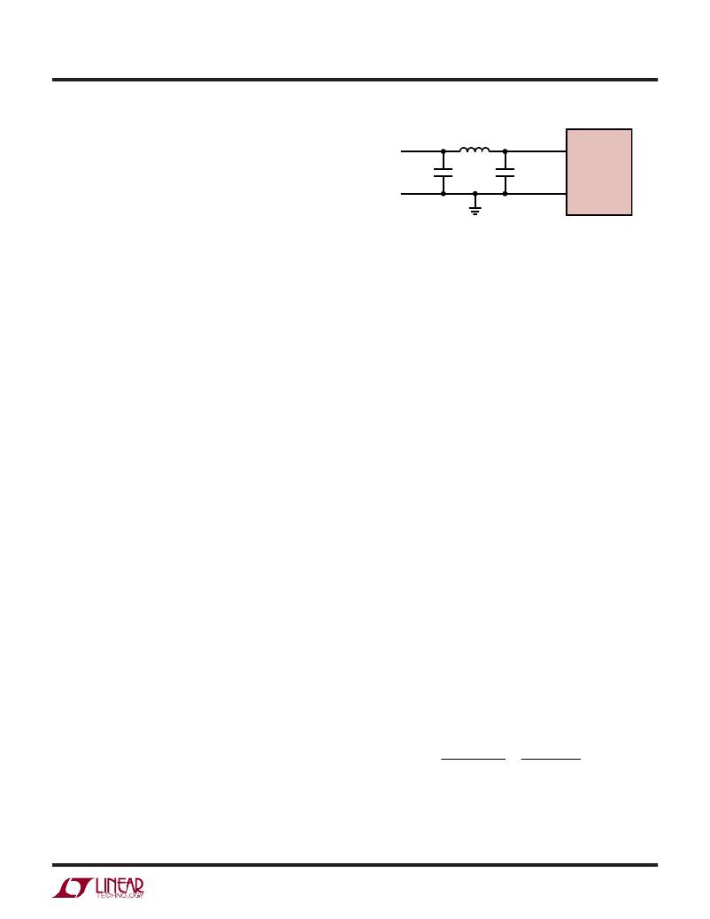
�Figure� 3.� 10nH� Inductor� Used� for�
�3240� F03�
�where� f� OSC� is� the� oscillator� frequency� (typically� 1.2MHz)�
�and� C� OUT� is� the� value� of� the� output� capacitor.�
�Also,� the� value� and� style� of� the� output� capacitor� can� sig-�
�ni?cantly� affect� the� stability� of� the� LTC3240.� As� shown�
�in� the� Block� Diagram,� the� LTC3240� uses� a� linear� control�
�loop� to� adjust� the� strength� of� the� charge� pump� to� match�
�the� current� required� at� the� output.� The� error� signal� of� this�
�loop� is� stored� directly� on� the� output� storage� capacitor.�
�This� output� capacitor� also� serves� to� form� the� dominant�
�pole� of� the� control� loop.� To� prevent� ringing� or� instability�
�on� the� LTC3240,� it� is� important� to� maintain� at� least� 2μF�
�of� capacitance� over� all� conditions.�
�Excessive� ESR� on� the� output� capacitor� can� degrade� the�
�loop� stability� of� the� LTC3240.� The� closed-loop� output�
�resistance� of� the� LTC3240� is� designed� to� be� 0.5� Ω� .� For� a�
�100mA� load� current� change,� the� output� voltage� will� change�
�by� about� 50mV.� If� the� output� capacitor� has� 0.5� Ω� or� more�
�of� ESR,� the� closed-loop� frequency� response� will� cease� to�
�roll� off� in� a� simple� one-pole� fashion� and� poor� load� transient�
�response� or� instability� could� result.� Ceramic� capacitors�
�typically� have� exceptional� ESR� performance� and� combined�
�with� a� tight� board� layout� should� yield� very� good� stability�
�and� load� transient� performance.�
�Just� as� the� value� of� C� OUT� controls� the� amount� of� output�
�ripple,� the� value� of� C� IN� controls� the� amount� of� ripple�
�present� at� the� input� pin� (V� IN� )� in� charge� pump� mode.� The�
�input� current� to� the� LTC3240� is� relatively� constant� during�
�the� input� charging� phase� and� the� output� charging� phase�
�Additional� Input� Noise� Reduction�
�Further� input� noise� reduction� can� be� achieved� by� power-�
�ing� the� LTC3240� through� a� very� small� series� inductor� as�
�shown� in� Figure� 3.� A� 10nH� inductor� will� reject� the� fast�
�current� notches,� thereby� presenting� a� nearly� constant�
�current� load� to� the� input� power� supply.� For� economy,� the�
�10nH� inductor� can� be� fabricated� on� the� PC� board� with�
�about� 1cm� (0.4")� of� PC� board� trace.�
�Flying� Capacitor� Selection�
�Warning:� A� polarized� capacitor� such� as� tantalum� or� alumi-�
�num� should� never� be� used� for� the� ?ying� capacitor� since�
�its� voltage� can� reverse� upon� start-up� of� the� LTC3240.�
�Low� ESR� ceramic� capacitors� should� always� be� used� for�
�the� ?ying� capacitor.�
�The� ?ying� capacitor� controls� the� strength� of� the� charge�
�pump.� A� 1μF� or� greater� ceramic� capacitor� is� suggested�
�for� the� ?ying� capacitor.� For� the� LTC3240-3.3� operating�
�at� an� input� voltage� in� the� range� 1.8V� ≤� V� IN� ≤� 2.5V,� it� is�
�necessary� to� have� at� least� 0.5μF� of� capacitance� for� the�
�?ying� capacitor� in� order� to� achieve� the� maximum� rated�
�current� of� 40mA.�
�For� very� light� load� applications,� the� ?ying� capacitor� may�
�be� reduced� to� save� space� or� cost.� From� the� ?rst� order�
�approximation� of� R� OL� in� the� “Effective� Open-Loop� Output�
�Resistance”� section,� the� theoretical� minimum� output�
�resistance� of� a� voltage� doubling� charge� pump� can� be�
�expressed� by� the� following� equation:�
�?�
�but� drops� to� zero� during� the� nonoverlap� times.� Since� the�
�nonoverlap� time� is� small� (~25ns),� these� missing� notches�
�result� in� a� small� perturbation� on� the� input� power� supply�
�R� OL� (� MIN� )� =�
�2� V� IN� –� V� OUT� 1�
�I� OUT� f� OSC� ?� C� FLY�
�line.� A� higher� ESR� capacitor� such� as� tantalum� will� have�
�higher� input� noise� than� a� low� ESR� ceramic� capacitor.�
�Therefore,� ceramic� capacitors� are� again� recommended�
�for� their� exceptional� ESR� performance.�
�where� f� OSC� is� the� switching� frequency� (1.2MHz)� and� C� FLY�
�is� the� value� of� the� ?ying� capacitor.� The� charge� pump�
�will� typically� be� weaker� than� the� theoretical� limit� due�
�3240fb�
�9�
�相关PDF资料 |
PDF描述 |
|---|---|
| LTC3250ES6-1.5#TRPBF | IC REG BUCK 1.5V 0.25A SOT23-6 |
| LTC3251EMSE-1.5#TRPBF | IC REG BUCK SWITCHED CAP 10MSOP |
| LTC3252EDE#TRPBF | IC REG BUCK SWITCHED CAP 12DFN |
| LTC3388IMSE-3#TRPBF | IC REG BUCK SYNC 50MA 10MSOP |
| LTC3400ES6-1#TRPBF | IC REG BST SYNC ADJ .85A SOT23-6 |
相关代理商/技术参数 |
参数描述 |
|---|---|
| LTC3240EDC-3.3 | 制造商:LINER 制造商全称:Linear Technology 功能描述:3.3V/2.5V Step-Up/ Step-Down Charge Pump DC/DC Converter |
| LTC3240EDC3.3#PBF | 制造商:Linear Technology 功能描述:Charge Pump STPUP/STPDN 3.3V 150mA 6-Pin DFN EP |
| LTC3240EDC-3.3#PBF | 制造商:Linear Technology 功能描述:DC-DC CONVERTER BUCK 1.22MHZ 制造商:Linear Technology 功能描述:DC-DC CONVERTER, BUCK, 1.22MHZ, 3.3V, 150mA, DFN-6; Primary Input Voltage:5.5V; No. of Outputs:1; Output Voltage:3.3V; Output Current:150mA; No. of Pins:6; Operating Temperature Min:-40C; Operating Temperature Max:85C ;RoHS Compliant: Yes |
| LTC3240EDC-3.3#TRMPBF | 功能描述:IC REG MULTI CONFIG 3.3V 6DFN RoHS:是 类别:集成电路 (IC) >> PMIC - 稳压器 - DC DC 开关稳压器 系列:- 产品培训模块:High Efficiency Current Mode Switching Regulators CMOS LDO Regulators 特色产品:BD91x Series Step-Down Regulators 标准包装:2,500 系列:- 类型:降压(降压) 输出类型:两者兼有 输出数:2 输出电压:3.3V,0.8 V ~ 2.5 V 输入电压:4.5 V ~ 5.5 V PWM 型:电流模式 频率 - 开关:1MHz 电流 - 输出:1.5A 同步整流器:是 工作温度:-40°C ~ 85°C 安装类型:表面贴装 封装/外壳:20-VFQFN 裸露焊盘 包装:带卷 (TR) 供应商设备封装:VQFN020V4040 产品目录页面:1373 (CN2011-ZH PDF) 其它名称:BD9152MUV-E2TR |
| LTC3240EDC-3.3#TRPBF | 功能描述:IC REG MULTI CONFIG 3.3V 6DFN RoHS:是 类别:集成电路 (IC) >> PMIC - 稳压器 - DC DC 开关稳压器 系列:- 标准包装:2,500 系列:- 类型:升压(升压) 输出类型:可调式 输出数:1 输出电压:1.24 V ~ 30 V 输入电压:1.5 V ~ 12 V PWM 型:电流模式,混合 频率 - 开关:600kHz 电流 - 输出:500mA 同步整流器:无 工作温度:-40°C ~ 85°C 安装类型:表面贴装 封装/外壳:8-SOIC(0.154",3.90mm 宽) 包装:带卷 (TR) 供应商设备封装:8-SOIC |
发布紧急采购,3分钟左右您将得到回复。