- 您现在的位置:买卖IC网 > PDF目录14530 > LTC3250ES6-1.5#TRM (Linear Technology)IC REG BUCK 1.5V 0.25A SOT23-6 PDF资料下载
参数资料
| 型号: | LTC3250ES6-1.5#TRM |
| 厂商: | Linear Technology |
| 文件页数: | 7/12页 |
| 文件大小: | 0K |
| 描述: | IC REG BUCK 1.5V 0.25A SOT23-6 |
| 标准包装: | 1 |
| 类型: | 降压(降压) |
| 输出类型: | 固定 |
| 输出数: | 1 |
| 输出电压: | 1.5V |
| 输入电压: | 3.1 V ~ 5.5 V |
| PWM 型: | Burst Mode? |
| 频率 - 开关: | 1.5MHz |
| 电流 - 输出: | 250mA |
| 同步整流器: | 无 |
| 工作温度: | -40°C ~ 85°C |
| 安装类型: | 表面贴装 |
| 封装/外壳: | SOT-23-6 |
| 包装: | 剪切带 (CT) |
| 供应商设备封装: | SOT-23-6 |
| 产品目录页面: | 1339 (CN2011-ZH PDF) |
| 其它名称: | LTC3250ES6-1.5 LTC3250ES6-1.5#TRMCT LTC3250ES6-1.5-ND |
�� �
�
�LTC3250-1.5/LTC3250-1.2�
�OPERATIO�
�(Refer� to� Simplified� Block� Diagram)�
�current.� For� an� ideal� 2� to� 1� step-down� charge� pump� the�
�power� efficiency� is� given� by:�
�0.15� ?� for� the� LTC3250-1.5� and� 0.12� ?� for� the�
�LTC3250-1.2.� For� a� 250mA� load� current� change� the� output�
�voltage� will� change� by� about� 37mV� for� the� LTC3250-1.5�
�=� =�
�η≡�
�P� OUT�
�P� IN�
�V� OUT� ?� I� OUT�
�1�
�V� IN� ?� I� OUT�
�2�
�2� V� OUT�
�V� IN�
�and� by� 30mV� for� the� LTC� 3250-1.2.� If� the� ESR� of� the� output�
�capacitor� is� greater� than� the� closed-loop-output� imped-�
�ance� the� part� will� cease� to� roll-off� in� a� simple� one-pole�
�fashion� and� poor� load� transient� response� or� instability�
�The� switching� losses� and� quiescent� current� of� the�
�LTC3250-1.5/LTC3250-1.2� are� designed� to� minimize� effi-�
�ciency� loss� over� the� entire� output� current� range,� causing�
�only� a� couple� %� error� from� the� theoritical� efficiency.� For�
�example� with� V� IN� =� 3.6V,� I� OUT� =� 100mA� and� V� OUT� regulat-�
�ing� to� 1.5V� the� measured� efficiency� is� 80.6%� which� is� in�
�close� agreement� with� the� theoretical� 83.3%� calculation.�
�V� OUT� Capacitor� Selection�
�could� result.� Ceramic� capacitors� typically� have� excep-�
�tional� ESR� performance� and� combined� with� a� tight� board�
�layout� should� yield� excellent� stability� and� load� transient�
�performance.�
�Further� output� noise� reduction� can� be� achieved� by� filtering�
�the� LTC3250-1.5/LTC3250-1.2� output� through� a� very� small�
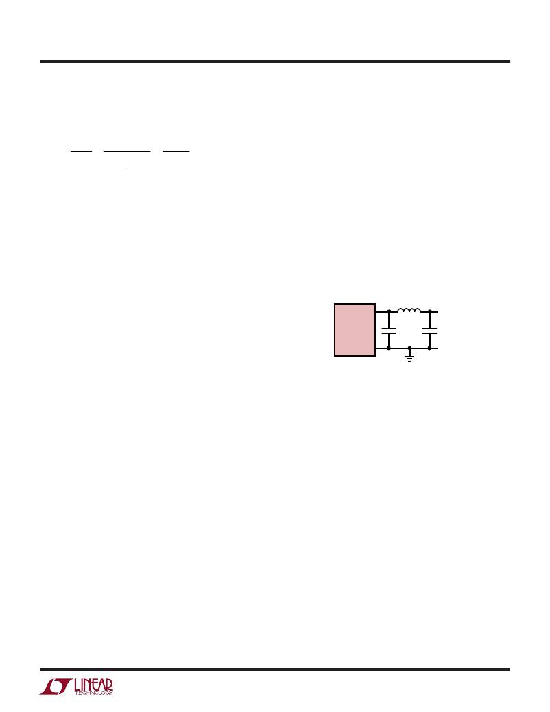
�series� inductor� as� shown� in� Figure� 1.� A� 10nH� inductor� will�
�10nH�
�The� ESR� and� value� of� capacitors� used� with� the� LTC3250-�
�1.5/LTC3250-1.2� determine� several� important� parameters�
�such� as� regulator� control� loop� stability,� output� ripple,� and�
�V� OUT�
�LTC3250-1.5/�
�LTC3250-1.2�
�(TRACE� INDUCTANCE)�
�4.7� μ� F�
�V� OUT�
�0.22� μ� F�
�charge� pump� strength.�
�The� value� of� C� OUT� directly� controls� the� amount� of� output�
�ripple� for� a� given� load� current.� Increasing� the� size� of� C� OUT�
�will� reduce� the� output� ripple.�
�To� reduce� output� noise� and� ripple,� it� is� suggested� that� a�
�low� ESR� (<0.1� ?� )� ceramic� capacitor� (4.7� μ� F� or� greater)� be�
�used� for� C� OUT� .� Tantalum� and� aluminum� capacitors� are� not�
�recommended� because� of� their� high� ESR.�
�Both� ESR� and� value� of� the� C� OUT� can� significantly� affect� the�
�stability� of� the� LTC3250-1.5/LTC3250-1.2.� As� shown� in�
�the� block� diagram,� the� LTC3250-1.5/LTC3250-1.2� use� a�
�control� loop� to� adjust� the� strength� of� the� charge� pump� to�
�match� the� current� required� at� the� output.� The� error� signal�
�of� this� loop� is� stored� directly� on� the� output� charge� storage�
�capacitor.� Thus� the� charge� storage� capacitor� also� serves�
�to� form� the� dominant� pole� for� the� control� loop.� To� prevent�
�ringing� or� instability� it� is� important� for� the� output� capacitor�
�to� maintain� at� least� 2.5� μ� F� of� capacitance� over� all� condi-�
�tions� (see� “Ceramic� Capacitor� Selection� Guidelines”� sec-�
�tion).�
�Likewise� excessive� ESR� on� the� output� capacitor� will� tend�
�to� degrade� the� loop� stability� of� the� LTC3250-1.5/LTC3250-�
�GND�
�3250� F01�
�Figure� 1.� 10nH� Inductor� Used� for�
�Additional� Output� Noise� Reduction�
�reject� the� fast� output� transients,� thereby� presenting� a�
�nearly� constant� output� voltage.� For� economy� the� 10nH�
�inductor� can� be� fabricated� on� the� PC� board� with� about� 1cm�
�(0.4")� of� PC� board� trace.�
�V� IN� Capacitor� Selection�
�The� constant� frequency� architecture� used� by� the�
�LTC3250-1.5/LTC3250-1.2� makes� input� noise� filtering�
�much� less� demanding� than� conventional� charge� pump�
�regulators.� On� a� cycle� by� cycle� basis,� the� LTC3250-1.5/�
�LTC3250-1.2� input� current� will� go� from� I� OUT� /2� to� 0mA.�
�Lower� ESR� will� reduce� the� voltage� steps� caused� by� chang-�
�ing� input� current,� while� the� absolute� capacitor� value� will�
�determine� the� level� of� ripple.� For� optimal� input� noise� and�
�ripple� reduction,� it� is� recommended� that� a� low� ESR� 1� μ� F� or�
�greater� ceramic� capacitor� be� used� for� C� IN� (see� “Ceramic�
�Capacitor� Selection� Guidelines”� section).� Aluminum� and�
�tantalum� capacitors� are� not� recommended� because� of�
�their� high� ESR.�
�1.2.� The� closed-loop� output� resistance� is� designed� to� be�
�3250fa�
�7�
�相关PDF资料 |
PDF描述 |
|---|---|
| VE-JNF-EX-S | CONVERTER MOD DC/DC 72V 75W |
| MAX860IUA+ | IC REG SWITCHD CAP DBL INV 8UMAX |
| RCA30DTKD-S288 | CONN EDGECARD 60POS .125 EXTEND |
| VE-JN0-EX-S | CONVERTER MOD DC/DC 5V 75W |
| 2200LL-102-H-RC | INDUCTOR TOROID 1000UH 15% HORIZ |
相关代理商/技术参数 |
参数描述 |
|---|---|
| LTC3251 | 制造商:LINER 制造商全称:Linear Technology 功能描述:500mA High Efficiency, Low Noise, Inductorless Step-Down DC/DC Converter |
| LTC3251-1.2 | 制造商:LINER 制造商全称:Linear Technology 功能描述:500mA High Efficiency, Low Noise, Inductorless Step-Down DC/DC Converter |
| LTC3251-1.5 | 制造商:LINER 制造商全称:Linear Technology 功能描述:500mA High Efficiency, Low Noise, Inductorless Step-Down DC/DC Converter |
| LTC3251EMSE | 功能描述:IC REG BUCK SWITCHED CAP 10MSOP RoHS:否 类别:集成电路 (IC) >> PMIC - 稳压器 - DC DC 开关稳压器 系列:- 标准包装:2,500 系列:- 类型:升压(升压) 输出类型:可调式 输出数:1 输出电压:1.24 V ~ 30 V 输入电压:1.5 V ~ 12 V PWM 型:电流模式,混合 频率 - 开关:600kHz 电流 - 输出:500mA 同步整流器:无 工作温度:-40°C ~ 85°C 安装类型:表面贴装 封装/外壳:8-SOIC(0.154",3.90mm 宽) 包装:带卷 (TR) 供应商设备封装:8-SOIC |
| LTC3251EMSE#PBF | 功能描述:IC REG BUCK SWITCHED CAP 10MSOP RoHS:是 类别:集成电路 (IC) >> PMIC - 稳压器 - DC DC 开关稳压器 系列:- 标准包装:250 系列:- 类型:降压(降压) 输出类型:固定 输出数:1 输出电压:1.2V 输入电压:2.05 V ~ 6 V PWM 型:电压模式 频率 - 开关:2MHz 电流 - 输出:500mA 同步整流器:是 工作温度:-40°C ~ 85°C 安装类型:表面贴装 封装/外壳:6-UFDFN 包装:带卷 (TR) 供应商设备封装:6-SON(1.45x1) 产品目录页面:1032 (CN2011-ZH PDF) 其它名称:296-25628-2 |
发布紧急采购,3分钟左右您将得到回复。