- 您现在的位置:买卖IC网 > PDF目录44990 > LTC3406ABES5#PBF (LINEAR TECHNOLOGY CORP) 1.3 A SWITCHING REGULATOR, 1800 kHz SWITCHING FREQ-MAX, PDSO5 PDF资料下载
参数资料
| 型号: | LTC3406ABES5#PBF |
| 厂商: | LINEAR TECHNOLOGY CORP |
| 元件分类: | 稳压器 |
| 英文描述: | 1.3 A SWITCHING REGULATOR, 1800 kHz SWITCHING FREQ-MAX, PDSO5 |
| 封装: | LEAD FREE, PLASTIC, MO-193, TSOT-23, 5 PIN |
| 文件页数: | 2/16页 |
| 文件大小: | 307K |
| 代理商: | LTC3406ABES5#PBF |
LTC3406AB
10
3406abfa
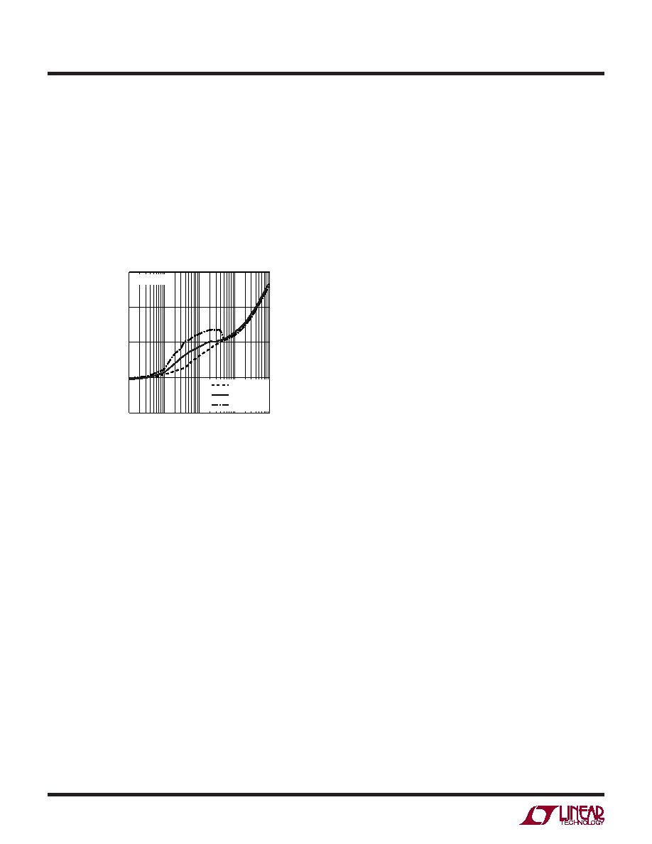
Although all dissipative elements in the circuit produce
losses, two main sources usually account for most of
the losses in LTC3406AB circuits: VIN quiescent current
and I2R losses. The VIN quiescent current loss dominates
the efciency loss at very low load currents whereas the
I2R loss dominates the efciency loss at medium to high
load currents. In a typical efciency plot, the efciency
curve at very low load currents can be misleading since
the actual power lost is of no consequence as illustrated
in Figure 2.
2. I2R losses are calculated from the resistances of the
internal switches, RSW, and external inductor RL. In
continuous mode, the average output current owing
through inductor L is “chopped” between the main
switch and the synchronous switch. Thus, the series
resistance looking into the SW pin is a function of both
top and bottom MOSFET RDS(ON) and the duty cycle
(DC) as follows:
RSW = (RDS(ON)TOP)(DC) + (RDS(ON)BOT)(1 – DC)
The RDS(ON)forboththetopandbottomMOSFETscanbe
obtained from the Typical Performance Characteristics
curves. Thus, to obtain I2R losses, simply add RSW to
RL and multiply the result by the square of the average
output current.
Other losses including CIN and COUT ESR dissipative losses
and inductor core losses generally account for less than
2% total additional loss.
Thermal Considerations
In most applications the LTC3406AB does not dissipate
much heat due to its high efciency. But, in applications
where the LTC3406AB is running at high ambient tem-
perature with low supply voltage and high duty cycles,
such as in dropout, the heat dissipated may exceed the
maximum junction temperature of the part. If the junction
temperature reaches approximately 150°C, both power
switches will be turned off and the SW node will become
high impedance.
To avoid the LTC3406AB from exceeding the maximum
junction temperature, the user will need to do some thermal
analysis. The goal of the thermal analysis is to determine
whether the power dissipated exceeds the maximum
junction temperature of the part. The temperature rise is
given by:
TR = (PD)(θJA)
where PD is the power dissipated by the regulator and θJA
is the thermal resistance from the junction of the die to
the ambient temperature.
APPLICATIONS INFORMATION
Figure 2. Power Lost vs Load Current
1. The VIN quiescent current is due to two components:
the DC bias current as given in the electrical charac-
teristics and the internal main switch and synchronous
switch gate charge currents. The gate charge current
results from switching the gate capacitance of the
internal power MOSFET switches. Each time the gate
is switched from high to low to high again, a packet of
charge, dQ, moves from VIN to ground. The resulting
dQ/dt is the current out of VIN that is typically larger
than the DC bias current. In continuous mode, IGATECHG
= f(QT + QB) where QT and QB are the gate charges of
the internal top and bottom switches. Both the DC bias
and gate charge losses are proportional to VIN and thus
their effects will be more pronounced at higher supply
voltages.
OUTPUT CURRENT (mA)
0.01
0.001
POWER
LOSS
(W)
0.1
10.0
100.0
1000.0
3406B F08
0.0001
1.0
1
VIN = 3.6V
VOUT = 1.2V
VOUT = 1.8V
VOUT = 2.5V
相关PDF资料 |
PDF描述 |
|---|---|
| LTC3406ABES5#TRM | 1.3 A SWITCHING REGULATOR, 1800 kHz SWITCHING FREQ-MAX, PDSO5 |
| LTC3406ABES5#TR | 1.3 A SWITCHING REGULATOR, 1800 kHz SWITCHING FREQ-MAX, PDSO5 |
| LTC3406B-2ES5#PBF | 1.3 A SWITCHING REGULATOR, 2700 kHz SWITCHING FREQ-MAX, PDSO5 |
| LTC3406BES5-1.2#PBF | 1.3 A SWITCHING REGULATOR, 1800 kHz SWITCHING FREQ-MAX, PDSO5 |
| LTC3407AEMSE#TR | 1.25 A DUAL SWITCHING CONTROLLER, 1800 kHz SWITCHING FREQ-MAX, PDSO10 |
相关代理商/技术参数 |
参数描述 |
|---|---|
| LTC3406ABES5TRMPBF | 制造商:Linear Technology 功能描述:DC-DC Converter Step-Down 5.5V TSOT23-5 |
| LTC3406ABES5-TRPBF | 制造商:LINER 制造商全称:Linear Technology 功能描述:1.5MHz, 600mA Synchronous Step-Down Regulator in ThinSOT |
| LTC3406AES5#TRMPBF | 功能描述:IC REG BUCK SYNC ADJ TSOT23-5 RoHS:是 类别:集成电路 (IC) >> PMIC - 稳压器 - DC DC 开关稳压器 系列:- 标准包装:250 系列:- 类型:降压(降压) 输出类型:固定 输出数:1 输出电压:1.2V 输入电压:2.05 V ~ 6 V PWM 型:电压模式 频率 - 开关:2MHz 电流 - 输出:500mA 同步整流器:是 工作温度:-40°C ~ 85°C 安装类型:表面贴装 封装/外壳:6-UFDFN 包装:带卷 (TR) 供应商设备封装:6-SON(1.45x1) 产品目录页面:1032 (CN2011-ZH PDF) 其它名称:296-25628-2 |
| LTC3406AES5#TRPBF | 功能描述:IC REG BUCK SYNC ADJ TSOT23-5 RoHS:是 类别:集成电路 (IC) >> PMIC - 稳压器 - DC DC 开关稳压器 系列:- 标准包装:2,500 系列:- 类型:升压(升压) 输出类型:可调式 输出数:1 输出电压:1.24 V ~ 30 V 输入电压:1.5 V ~ 12 V PWM 型:电流模式,混合 频率 - 开关:600kHz 电流 - 输出:500mA 同步整流器:无 工作温度:-40°C ~ 85°C 安装类型:表面贴装 封装/外壳:8-SOIC(0.154",3.90mm 宽) 包装:带卷 (TR) 供应商设备封装:8-SOIC |
| LTC3406AES5-PBF | 制造商:LINER 制造商全称:Linear Technology 功能描述:1.5MHz, 600mA Synchronous Step-Down Regulator in ThinSOT |
发布紧急采购,3分钟左右您将得到回复。