- 您现在的位置:买卖IC网 > PDF目录69007 > LTC3407IMSE-2#TR (LINEAR TECHNOLOGY CORP) 1.6 A DUAL SWITCHING CONTROLLER, 2700 kHz SWITCHING FREQ-MAX, PDSO10 PDF资料下载
参数资料
| 型号: | LTC3407IMSE-2#TR |
| 厂商: | LINEAR TECHNOLOGY CORP |
| 元件分类: | 稳压器 |
| 英文描述: | 1.6 A DUAL SWITCHING CONTROLLER, 2700 kHz SWITCHING FREQ-MAX, PDSO10 |
| 封装: | PLASTIC, MSOP-10 |
| 文件页数: | 13/16页 |
| 文件大小: | 227K |
| 代理商: | LTC3407IMSE-2#TR |
LTC3407-2
6
34072fb
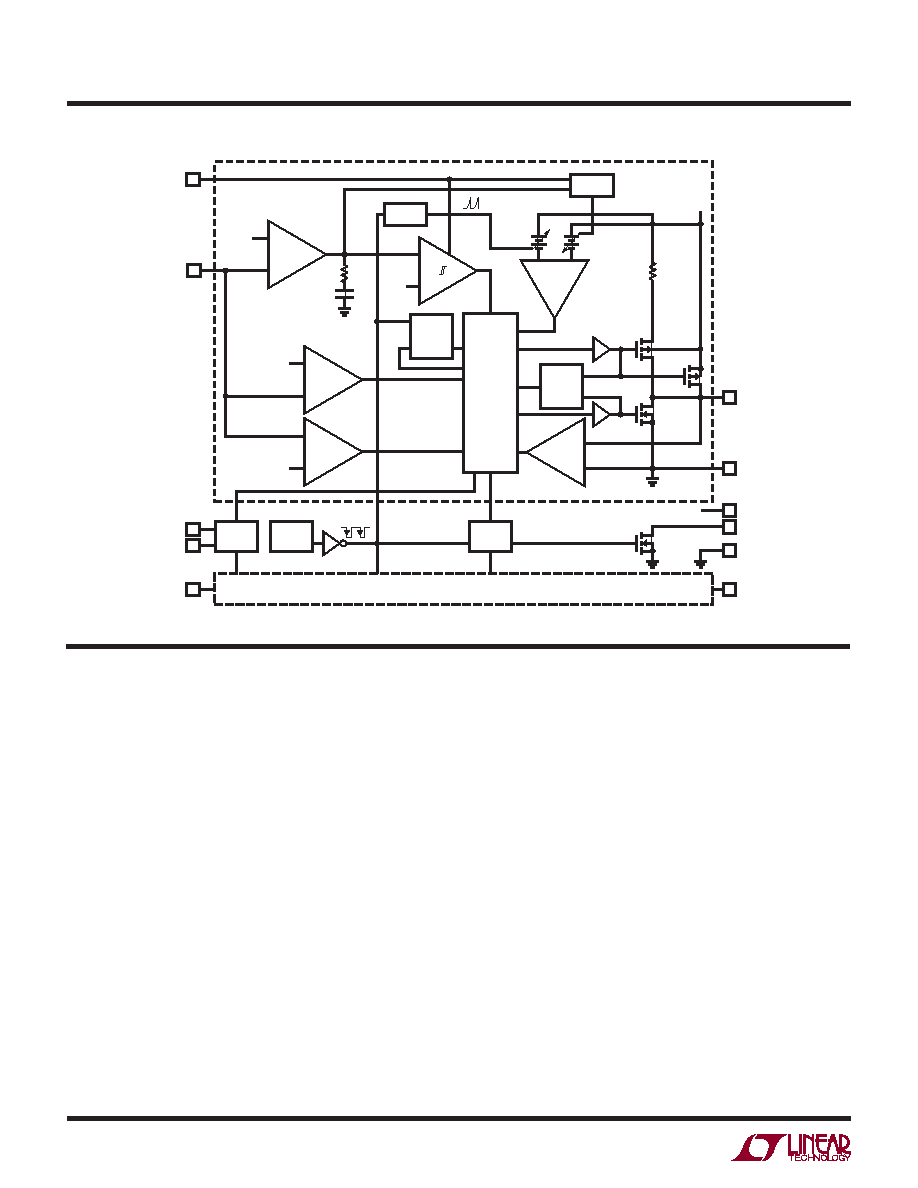
BLOCK DIAGRAM
OPERATION
1
2
9
10
8
3
4
11
5
–
+
–
+
–
+
–
+
EA
UVDET
OVDET
0.6V
7
0.65V
0.55V
–
+
0.35V
UV
OV
ITH
SWITCHING
LOGIC
AND
BLANKING
CIRCUIT
S
R
Q
RS
LATCH
BURST
–
+
ICOMP
IRCMP
ANTI
SHOOT-
THRU
BURST
CLAMP
SLOPE
COMP
EN
SLEEP
POR
COUNTER
0.6V REF
OSC
REGULATOR 2 (IDENTICAL TO REGULATOR 1)
PGOOD1
PGOOD2
SHUTDOWN
VIN
6
REGULATOR 1
SW1
GND
POR
GND
SW2
5
MODE/SYNC
VFB1
RUN1
RUN2
VFB2
34072 BD
The LTC3407-2 uses a constant-frequency, current mode
architecture. The operating frequency is set at 2.25MHz
and can be synchronized to an external oscillator. Both
channels share the same clock and run in-phase. To suit a
variety of applications, the selectable Mode pin allows the
user to choose between low noise and high efciency.
The output voltage is set by an external divider returned
to the VFB pins. An error amplier compares the divided
output voltage with a reference voltage of 0.6V and adjusts
the peak inductor current accordingly. Overvoltage and
undervoltage comparators will pull the POR output low if
the output voltage is not within ±8.5%. The POR output
will go high after 262,144 clock cycles (about 117ms) of
achieving regulation.
Main Control Loop
During normal operation, the top power switch (P-channel
MOSFET) is turned on at the beginning of a clock cycle
when the VFB voltage is below the the reference voltage.
The current into the inductor and the load increases until
the current limit is reached. The switch turns off and
energy stored in the inductor ows through the bottom
switch (N-channel MOSFET) into the load until the next
clock cycle.
The peak inductor current is controlled by the internally
compensated ITH voltage, which is the output of the er-
ror amplier.This amplier compares the VFB pin to the
0.6V reference. When the load current increases, the
VFB voltage decreases slightly below the reference. This
decrease causes the error amplier to increase the ITH
voltage until the average inductor current matches the
new load current.
The main control loop is shut down by pulling the RUN
pin to ground.
相关PDF资料 |
PDF描述 |
|---|---|
| LTC3528BEDDB#TRM | SWITCHING REGULATOR, 1300 kHz SWITCHING FREQ-MAX, PDSO8 |
| LTC3528EDDB#TRM | SWITCHING REGULATOR, 1300 kHz SWITCHING FREQ-MAX, PDSO8 |
| LTC3542EDC-1#PBF | SWITCHING REGULATOR, 2700 kHz SWITCHING FREQ-MAX, PDSO6 |
| LTC3547BIDDB#TRM | 0.7 A DUAL SWITCHING CONTROLLER, 2700 kHz SWITCHING FREQ-MAX, PDSO8 |
| LTC3547BEDDB-1#PBF | 0.7 A DUAL SWITCHING CONTROLLER, 2700 kHz SWITCHING FREQ-MAX, PDSO8 |
相关代理商/技术参数 |
参数描述 |
|---|---|
| LTC3408 | 制造商:LINER 制造商全称:Linear Technology 功能描述:1.5MHz, 600mA Synchronous Step-Down Regulator with Bypass Transistor |
| LTC3408EDD | 功能描述:IC REG BUCK W/BYPASS TXRX 8-DFN RoHS:否 类别:集成电路 (IC) >> PMIC - 稳压器 - 专用型 系列:- 标准包装:43 系列:- 应用:控制器,Intel VR11 输入电压:5 V ~ 12 V 输出数:1 输出电压:0.5 V ~ 1.6 V 工作温度:-40°C ~ 85°C 安装类型:表面贴装 封装/外壳:48-VFQFN 裸露焊盘 供应商设备封装:48-QFN(7x7) 包装:管件 |
| LTC3408EDD#PBF | 功能描述:IC REG BUCK W/BYPASS TXRX 8-DFN RoHS:是 类别:集成电路 (IC) >> PMIC - 稳压器 - 专用型 系列:- 标准包装:43 系列:- 应用:控制器,Intel VR11 输入电压:5 V ~ 12 V 输出数:1 输出电压:0.5 V ~ 1.6 V 工作温度:-40°C ~ 85°C 安装类型:表面贴装 封装/外壳:48-VFQFN 裸露焊盘 供应商设备封装:48-QFN(7x7) 包装:管件 |
| LTC3408EDD#TR | 功能描述:IC REG BUCK W/BYPASS TXRX 8-DFN RoHS:否 类别:集成电路 (IC) >> PMIC - 稳压器 - 专用型 系列:- 标准包装:43 系列:- 应用:控制器,Intel VR11 输入电压:5 V ~ 12 V 输出数:1 输出电压:0.5 V ~ 1.6 V 工作温度:-40°C ~ 85°C 安装类型:表面贴装 封装/外壳:48-VFQFN 裸露焊盘 供应商设备封装:48-QFN(7x7) 包装:管件 |
| LTC3408EDD#TRPBF | 功能描述:IC REG BUCK W/BYPASS TXRX 8-DFN RoHS:是 类别:集成电路 (IC) >> PMIC - 稳压器 - 专用型 系列:- 标准包装:43 系列:- 应用:控制器,Intel VR11 输入电压:5 V ~ 12 V 输出数:1 输出电压:0.5 V ~ 1.6 V 工作温度:-40°C ~ 85°C 安装类型:表面贴装 封装/外壳:48-VFQFN 裸露焊盘 供应商设备封装:48-QFN(7x7) 包装:管件 |
发布紧急采购,3分钟左右您将得到回复。