- 您现在的位置:买卖IC网 > PDF目录1829 > LTC3408EDD#TRPBF (Linear Technology)IC REG BUCK W/BYPASS TXRX 8-DFN PDF资料下载
参数资料
| 型号: | LTC3408EDD#TRPBF |
| 厂商: | Linear Technology |
| 文件页数: | 10/12页 |
| 文件大小: | 0K |
| 描述: | IC REG BUCK W/BYPASS TXRX 8-DFN |
| 标准包装: | 2,500 |
| 应用: | 转换器,WCDMA 功率放大器应用 |
| 输入电压: | 2.5 V ~ 5 V |
| 输出数: | 1 |
| 输出电压: | 0.3 V ~ 3.5 V |
| 工作温度: | -40°C ~ 85°C |
| 安装类型: | 表面贴装 |
| 封装/外壳: | 8-WFDFN 裸露焊盘 |
| 供应商设备封装: | 8-DFN-EP(3x3) |
| 包装: | 带卷 (TR) |
�� �
�
�LTC3408�
�APPLICATIO� S� I� FOR� ATIO�
�1�
�0.1�
�0.01�
�100�
�90�
�80�
�70�
�60�
�50�
�40�
�30�
�junction� temperature� of� the� part.� If� the� junction� tempera-�
�ture� reaches� approximately� 150� °� C,� both� power� switches�
�will� be� turned� off� and� the� SW� node� will� become� high�
�impedance.�
�To� prevent� the� LTC3408� from� exceeding� the� maximum�
�junction� temperature,� the� user� will� need� to� do� some�
�thermal� analysis.� The� goal� of� the� thermal� analysis� is� to�
�0.01�
�1�
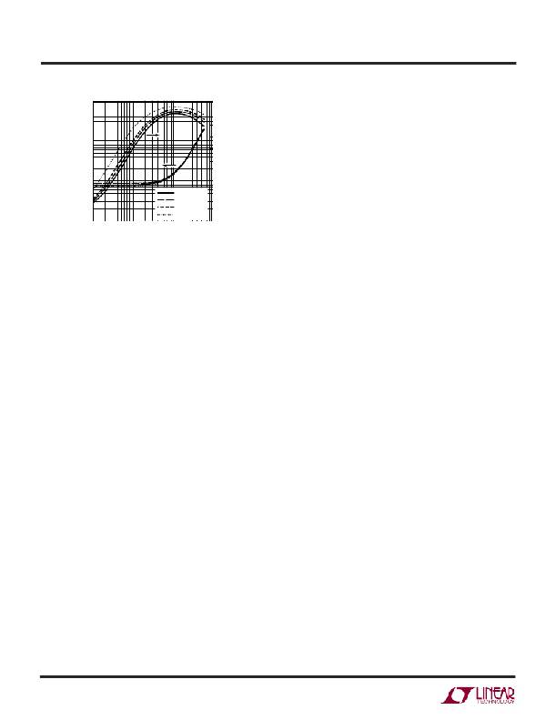
�V� OUT� =� 1.2V�
�V� OUT� =� 1.5V�
�V� OUT� =� 1.8V�
�V� OUT� =� 2.5V�
�10� 100�
�20�
�10�
�0�
�1000�
�determine� whether� the� power� dissipated� exceeds� the�
�maximum� junction� temperature� of� the� part.� The� tempera-�
�ture� rise� is� given� by:�
�LOAD� CURRENT� (mA)�
�3408� F04�
�T� R� =� (PD)(� θ� JA� )�
�Figure� 4.� Power� Lost� vs� Load� Current�
�I� GATECHG� =� f(Q� T� +� Q� B� ),� where� Q� T� and� Q� B� are� the� gate�
�charges� of� the� internal� top� and� bottom� switches.� Both� the�
�DC� bias� and� gate� charge� losses� are� proportional� to� V� IN� ,�
�thus,� their� effects� will� be� more� pronounced� at� higher�
�supply� voltages.� (The� gate� charge� of� the� bypass� FET� is,�
�of� course,� negligible� because� it� is� infrequently� cycled.)�
�2.� I� 2� R� losses� are� calculated� from� the� resistances� of� the�
�internal� switches,� R� SW� ,� and� external� inductor� R� L� .� In� con-�
�tinuous� mode,� the� average� output� current� flowing� through�
�inductor� L� is� “chopped”� between� the� main� switch� and� the�
�synchronous� switch.� Thus,� the� series� resistance� looking�
�into� the� SW� pin� is� a� function� of� both� top� and� bottom�
�MOSFET� R� DS(ON)� and� the� duty� cycle� (DC)� as� follows:�
�R� SW� =� (R� DS(ON)TOP� )(DC)� +� (R� DS(ON)BOT� )(1� –� DC)�
�The� R� DS(ON)� for� both� the� top� and� bottom� MOSFETs� can� be�
�obtained� from� the� Typical� Performance� Charateristics�
�curves.� Hence,� to� obtain� I� 2� R� losses,� simply� add� R� SW� to� R� L�
�and� multiply� the� result� by� the� square� of� the� average� output�
�current.�
�Other� losses� including� C� IN� and� C� OUT� ESR� dissipative�
�losses� and� inductor� core� losses� generally� account� for� less�
�than� 2%� total� additional� loss.�
�Thermal� Considerations�
�In� most� applications� the� LTC3408� does� not� dissipate�
�much� heat� due� to� its� high� efficiency.� But,� in� applications�
�where� the� LTC3408� is� running� at� high� ambient� tempera-�
�ture� with� low� supply� voltage� and� high� duty� cycles,� such� as�
�in� dropout,� the� heat� dissipated� may� exceed� the� maximum�
�where� PD� is� the� power� dissipated� by� the� regulator� and� θ� JA�
�is� the� thermal� resistance� from� the� junction� of� the� die� to� the�
�ambient� temperature.�
�The� junction� temperature,� T� J� ,� is� given� by:�
�T� J� =� T� A� +� T� R�
�where T� A� is the ambient temperature.�
�As� an� example,� consider� the� LTC3408� in� dropout� at� an�
�input� voltage� of� 2.7V,� a� load� current� of� 600mA� (0.9V� ≤� V� REF�
�<� 1.2V)� and� an� ambient� temperature� of� 70� °� C.� With� V� REF� <�
�1.2V,� the� entire� 600mA� flows� through� the� main� P-channel�
�FET.� From� the� typical� performance� graph� of� switch� resis-�
�tance,� the� R� DS(ON)� of� the� P-channel� switch� at� 70� °� C� is�
�approximately� 0.52� ?� .� Therefore,� power� dissipated� by� the�
�part� is:�
�PD� =� (I� LOAD2� )� ?� R� DS(ON)� =� 187.2mW�
�For� the� 8L� DFN� package,� the� θ� JA� is� 43� °� C/W.� Thus,� the�
�junction� temperature� of� the� regulator� is:�
�T� J� =� 70� °� C� +� (0.1872)(43)� =� 78� °� C�
�which� is� below� the� maximum� junction� temperature� of�
�125� °� C.�
�Modifying� this� example,� suppose� that� V� REF� is� raised� to�
�1.2V� or� higher.� This� turns� on� the� bypass� P-channel� FET� as�
�well� as� the� main� P-channel� FET.� Assume� that� the� inductor’s�
�DC� resistance� is� 0.1� ?� ,� the� R� DS(ON)� of� the� main� P-channel�
�switch� is� 0.52� ?� ,� and� the� R� DS(ON)� of� the� bypass� P-channel�
�switch� is� 0.08� ?� .� The� current� through� the� P-channel� switch�
�and� the� inductor� will� be� 69mA,� causing� power� dissipation�
�of� (0.069A)� 2� ?� 0.62� ?� =� 2.9mW.� The� bypass� FET� will�
�3408f�
�10�
�相关PDF资料 |
PDF描述 |
|---|---|
| LTC3409IDD#TRPBF | IC REG BUCK SYNC ADJ 0.6A 8DFN |
| LTC3410BESC6-1.8#TRPBF | IC REG BUCK SYNC 1.8V .3A SC70-6 |
| LTC3411AIMS#TRPBF | IC REG BUCK SYNC ADJ 10MSOP |
| LTC3411IMS#TRPBF | IC REG BUCK SYNC ADJ 10MSOP |
| LTC3412IFE#TRPBF | IC REG BUCK SYNC ADJ 16TSSOP |
相关代理商/技术参数 |
参数描述 |
|---|---|
| LTC3409 | 制造商:LINER 制造商全称:Linear Technology 功能描述:600mA Low Vin Buck Regulator in 3mm x 3mm DFN |
| LTC3409A | 制造商:LINER 制造商全称:Linear Technology 功能描述:600mA Low VIN Buck Regulator in 3mm × 3mm DFN |
| LTC3409AEDD | 制造商:LINER 制造商全称:Linear Technology 功能描述:600mA Low VIN Buck Regulator in 3mm × 3mm DFN |
| LTC3409AEDD#PBF | 功能描述:IC REG BUCK SYNC ADJ 0.6A 8DFN RoHS:是 类别:集成电路 (IC) >> PMIC - 稳压器 - DC DC 开关稳压器 系列:- 标准包装:2,500 系列:- 类型:升压(升压) 输出类型:可调式 输出数:1 输出电压:1.24 V ~ 30 V 输入电压:1.5 V ~ 12 V PWM 型:电流模式,混合 频率 - 开关:600kHz 电流 - 输出:500mA 同步整流器:无 工作温度:-40°C ~ 85°C 安装类型:表面贴装 封装/外壳:8-SOIC(0.154",3.90mm 宽) 包装:带卷 (TR) 供应商设备封装:8-SOIC |
| LTC3409AEDD#TRPBF | 功能描述:IC REG BUCK SYNC ADJ 0.6A 8DFN RoHS:是 类别:集成电路 (IC) >> PMIC - 稳压器 - DC DC 开关稳压器 系列:- 标准包装:2,500 系列:- 类型:升压(升压) 输出类型:可调式 输出数:1 输出电压:1.24 V ~ 30 V 输入电压:1.5 V ~ 12 V PWM 型:电流模式,混合 频率 - 开关:600kHz 电流 - 输出:500mA 同步整流器:无 工作温度:-40°C ~ 85°C 安装类型:表面贴装 封装/外壳:8-SOIC(0.154",3.90mm 宽) 包装:带卷 (TR) 供应商设备封装:8-SOIC |
发布紧急采购,3分钟左右您将得到回复。