- 您现在的位置:买卖IC网 > PDF目录13913 > LTC3413EFE (Linear Technology)IC REG BUCK SYNC ADJ 3A 16TSSOP PDF资料下载
参数资料
| 型号: | LTC3413EFE |
| 厂商: | Linear Technology |
| 文件页数: | 5/16页 |
| 文件大小: | 0K |
| 描述: | IC REG BUCK SYNC ADJ 3A 16TSSOP |
| 标准包装: | 95 |
| 类型: | 降压(降压) |
| 输出类型: | 可调式 |
| 输出数: | 1 |
| 输出电压: | 0.7 V ~ 5.5 V |
| 输入电压: | 2.25 V ~ 5.5 V |
| PWM 型: | 电流模式 |
| 频率 - 开关: | 1MHz |
| 电流 - 输出: | 3A |
| 同步整流器: | 是 |
| 工作温度: | -40°C ~ 85°C |
| 安装类型: | 表面贴装 |
| 封装/外壳: | 16-TSSOP(0.173",4.40mm)裸露焊盘 |
| 包装: | 管件 |
| 供应商设备封装: | 16-TSSOP-EP |
�� �
�
�LTC3413�
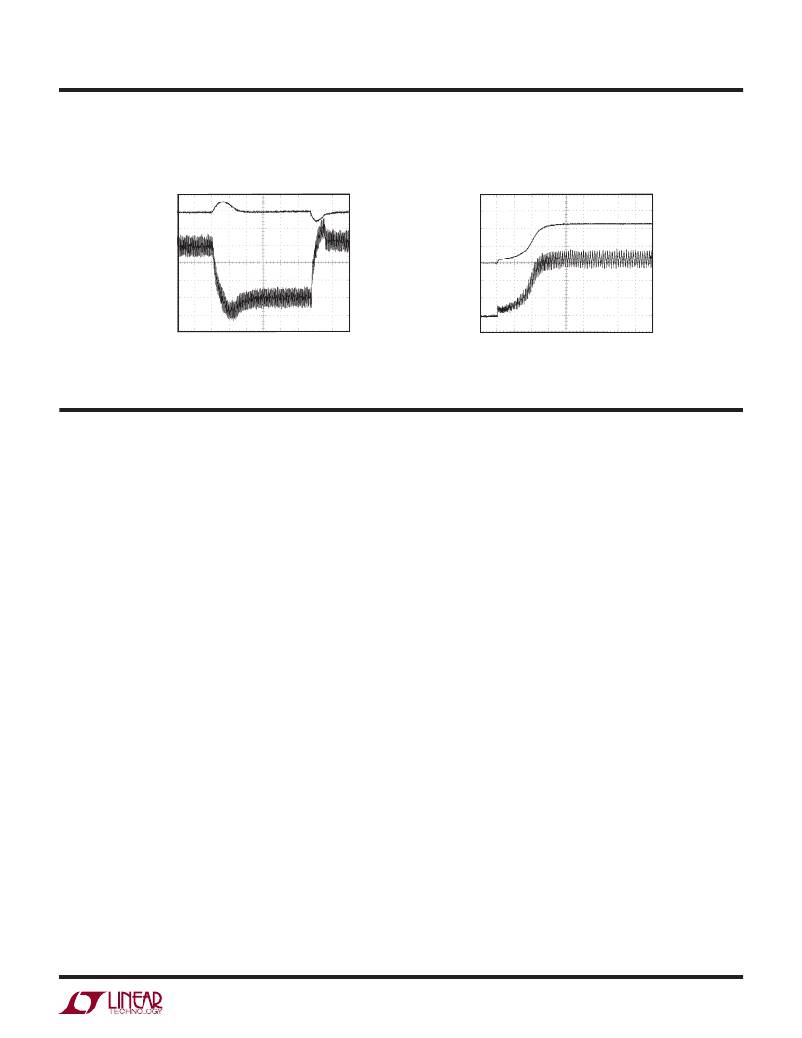
�TYPICAL� PERFORMANCE� CHARACTERISTICS�
�OUTPUT�
�VOLTAGE�
�100mV/DIV�
�Load� Step� Transient�
�OUTPUT�
�VOLTAGE�
�500mV/DIV�
�Start-Up�
�INDUCTOR�
�CURRENT�
�1A/DIV�
�INDUCTOR�
�CURRENT�
�1A/DIV�
�V� IN� =� 2.5V� 20μs/DIV�
�V� OUT� =� 1.25V�
�LOAD� STEP� =� 0A� TO� –3A�
�3413� G12�
�V� IN� =� 2.5V�
�V� OUT� =� 1.25V�
�LOAD� =� 0.4Ω�
�1ms/DIV�
�3413� G13�
�PIN� FUNCTIONS�
�SV� IN� (Pin� 1):� Signal� Input� Supply.� Decouple� this� pin� to�
�SGND� with� a� capacitor.� SV� IN� must� be� greater� or� equal� to�
�PV� IN� ,� however,� the� difference� between� SV� IN� and� PV� IN� must�
�be� less� than� 0.5V.�
�PGOOD� (Pin� 2):� Power� Good� Output.� Open-drain� logic�
�output� that� is� pulled� to� ground� when� the� output� voltage�
�is� not� within� ±10%� of� regulation� point.�
�I� TH� (Pin� 3):� Error� Ampli?er� Compensation� Point.� The�
�current� comparator� threshold� increases� with� this� control�
�voltage.� Nominal� voltage� range� for� this� pin� is� from� 0.2V�
�to� 1.4V� with� 0.6V� corresponding� to� the� zero-sense� voltage�
�(zero� current).�
�V� FB� (Pin� 4):� Feedback� Pin.� Receives� the� feedback� voltage�
�from� the� output.�
�R� T� (Pin� 5):� Oscillator� Resistor� Input.� Connecting� a� resistor�
�to� ground� from� this� pin� sets� the� switching� frequency.�
�V� REF� (Pin� 6):� Reference� Voltage� Input.� The� positive� input�
�RUN/SS� (Pin� 7):� Run� Control� and� Soft-Start� Input.� Forcing�
�this� pin� below� 0.5V� shuts� down� the� LTC3413.� In� shutdown�
�all� functions� are� disabled� drawing� <� 1μA� of� supply� current.�
�A� capacitor� to� ground� from� this� pin� sets� the� ramp� time� to�
�full� output� current.�
�SGND� (Pin� 8):� Signal� Ground.� All� small-signal� components�
�and� compensation� components� should� connect� to� this�
�ground,� which� in� turn� connects� to� PGND� at� one� point.�
�PV� IN� (Pins� 9,� 16):� Power� Input� Supply.� Decouple� this� pin�
�to� PGND� with� a� capacitor.�
�SW� (Pins� 10,� 11,� 14,� 15):� Switch� Node� Connection� to�
�Inductor.� This� pin� connects� to� the� drains� of� the� internal�
�main� and� synchronous� power� MOSFET� switches.�
�PGND� (Pins� 12,� 13):� Power� Ground.� Connect� this� pin�
�closely� to� the� (–)� terminal� of� C� IN� and� C� OUT� .�
�Exposed� Pad� (Pin� 17):� Should� be� connected� to� PCB�
�ground.�
�of� the� internal� error� ampli?er� senses� one-half� of� the� volt-�
�age� at� this� pin� through� a� resistor� divider.�
�3413fc�
�5�
�相关PDF资料 |
PDF描述 |
|---|---|
| V300B5C150BG2 | CONVERTER MOD DC/DC 5V 150W |
| HM53-20171HLF | HIGH POWER LOW COST INDUCTORS |
| LT3641EFE#TRPBF | IC REG BUCK SYNC ADJ DL 28TSSOP |
| EBM36DCCD-S189 | CONN EDGECARD 72POS R/A .156 SLD |
| LTC3616EUDD#TRPBF | IC REG BUCK SYNC ADJ 6A 24QFN |
相关代理商/技术参数 |
参数描述 |
|---|---|
| LTC3413EFE#PBF | 功能描述:IC REG BUCK SYNC ADJ 3A 16TSSOP RoHS:是 类别:集成电路 (IC) >> PMIC - 稳压器 - DC DC 开关稳压器 系列:- 标准包装:250 系列:- 类型:降压(降压) 输出类型:固定 输出数:1 输出电压:1.2V 输入电压:2.05 V ~ 6 V PWM 型:电压模式 频率 - 开关:2MHz 电流 - 输出:500mA 同步整流器:是 工作温度:-40°C ~ 85°C 安装类型:表面贴装 封装/外壳:6-UFDFN 包装:带卷 (TR) 供应商设备封装:6-SON(1.45x1) 产品目录页面:1032 (CN2011-ZH PDF) 其它名称:296-25628-2 |
| LTC3413EFE#TR | 功能描述:IC REG BUCK SYNC ADJ 3A 16TSSOP RoHS:否 类别:集成电路 (IC) >> PMIC - 稳压器 - DC DC 开关稳压器 系列:- 设计资源:Design Support Tool 标准包装:1 系列:- 类型:升压(升压) 输出类型:固定 输出数:1 输出电压:3V 输入电压:0.75 V ~ 2 V PWM 型:- 频率 - 开关:- 电流 - 输出:100mA 同步整流器:是 工作温度:-40°C ~ 85°C 安装类型:表面贴装 封装/外壳:SOT-23-5 细型,TSOT-23-5 包装:剪切带 (CT) 供应商设备封装:TSOT-23-5 其它名称:AS1323-BTTT-30CT |
| LTC3413EFE#TRPBF | 功能描述:IC REG BUCK SYNC ADJ 3A 16TSSOP RoHS:是 类别:集成电路 (IC) >> PMIC - 稳压器 - DC DC 开关稳压器 系列:- 设计资源:Design Support Tool 标准包装:1 系列:- 类型:升压(升压) 输出类型:固定 输出数:1 输出电压:3V 输入电压:0.75 V ~ 2 V PWM 型:- 频率 - 开关:- 电流 - 输出:100mA 同步整流器:是 工作温度:-40°C ~ 85°C 安装类型:表面贴装 封装/外壳:SOT-23-5 细型,TSOT-23-5 包装:剪切带 (CT) 供应商设备封装:TSOT-23-5 其它名称:AS1323-BTTT-30CT |
| LTC3413EFEPBF | 制造商:Linear Technology 功能描述: 制造商:Linear Technology 功能描述:3A 2MHz Reg. for DDR Termination TSSOP16 |
| LTC3413EFE-PBF | 制造商:LINER 制造商全称:Linear Technology 功能描述:3A, 2MHz Monolithic Synchronous Regulator for DDR/QDR Memory Termination |
发布紧急采购,3分钟左右您将得到回复。