- 您现在的位置:买卖IC网 > PDF目录79678 > LTC3525ESC6-3#TRMPBF (LINEAR TECHNOLOGY CORP) 0.45 A SWITCHING REGULATOR, PDSO6 PDF资料下载
参数资料
| 型号: | LTC3525ESC6-3#TRMPBF |
| 厂商: | LINEAR TECHNOLOGY CORP |
| 元件分类: | 稳压器 |
| 英文描述: | 0.45 A SWITCHING REGULATOR, PDSO6 |
| 封装: | LEAD FREE, PLASTIC, MO-203AB, EIAJ, SC-70, 6 PIN |
| 文件页数: | 13/14页 |
| 文件大小: | 536K |
| 代理商: | LTC3525ESC6-3#TRMPBF |
LTC3525-3/
LTC3525-3.3/LTC3525-5
8
3525fb
The LTC3525 is a high performance Burst Mode operation
only, synchronous boost converter requiring only three
small external components. Its simplicity and small size
makeitahighefficiencyalternativetochargepumpdesigns.
It is designed to start up from a single alkaline or nickel
cell, with input voltages as low as 1V, or from two or three
cells (or a Li-Ion battery), with voltages as high as 4.5V.
Once started, VIN can be as low as 0.5V (depending on
load current) and maintain regulation. The output voltage
is preset internally to either 3V, 3.3V or 5V. Peak switch
currentis400mAminimum,providingregulationwithload
currents up to 150mA, depending on input voltage.
Synchronous rectification provides high efficiency opera-
tion while eliminating the need for an external Schottky
diode. True output disconnect eliminates inrush current
at start-up, and allows VOUT to be disconnected from VIN,
for zero shutdown current.
The output disconnect feature also allows the LTC3525 to
maintainregulationwithaninputvoltageequaltoorgreater
than VOUT. Note, however, that the synchronous rectifier
is not enabled in this mode resulting in lower efficiency
and reduced output current capability.
The operating quiescent current is only 7A typical, allow-
ing the converter to maintain high efficiency at extremely
light loads.
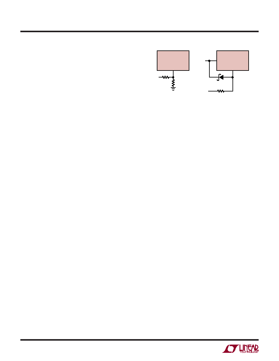
Shutdown
The LTC3525 is shut down by pulling SHDN below 0.4V,
and made active by raising it above 1V. Although SHDN can
be driven above VIN or VOUT (up to the absolute maximum
rating)withoutdamage,theLTC3525hasaproprietarytest
mode that may be engaged if SHDN is held in the range
of 0.5V to 1V higher than the greater of VIN or VOUT. If
the test mode is engaged, normal PWM switching action
is interrupted, which can cause undesirable operation
in some applications. Therefore, in applications where
SHDN may be driven above VIN, a resistor divider or other
means must be employed to keep the SHDN voltage below
(VIN + 0.4V) to prevent the possibility of the test mode
being engaged. Please refer to Figure 1 for two possible
implementations.
After the SHDN pin rises, there is a short delay before
switching starts. The delay is 20s to 120s, depending
on input voltage (see Typical Performance Characteristics
curve).
Start-Up
A start-up oscillator allows the LTC3525 to start with input
voltages as low as 1V. It remains in start-up mode until
two conditions are met. VOUT must exceed VIN by at least
0.2V typical and either VIN or VOUT must be greater than
1.8V typical.
During start-up, the synchronous rectifier is not enabled,
and the internal P-channel synchronous rectifier acts as
a follower, causing the peak voltage on SW to reach (VIN
+ 1V) typical. This limits inrush current by maintaining
control of the inductor current when VOUT is less than VIN.
ToreducepowerdissipationintheP-channelsynchronous
rectifier when the output is shorted, a foldback feature is
incorporated that reduces the peak inductor current when
VIN is more than 1.7V greater than VOUT.
Normal Operation
Once VOUT has increased more than 0.2V typical above
VIN, and either voltage is above 1.8V, normal operation
begins, with synchronous rectification enabled. In this
mode, the internal N-channel MOSFET connected be-
tween SW and GND stays on until the inductor current
reaches a maximum peak value, after which it is turned
off and the P-channel synchronous rectifier is turned
on. It stays on, delivering current to the output, until the
inductor current has dropped below a minimum value at
OPERATION
LTC3525
1M
VCNTRL
R
VIN
VCNTRL
SHDN
LTC3525
1M
3525 F01
ZETEX ZC2811E
R > (VCNTRL/(VIN + 0.4) – 1) M
SHDN
Figure 1
相关PDF资料 |
PDF描述 |
|---|---|
| LM236ZAP | 1-OUTPUT TWO TERM VOLTAGE REFERENCE, 2.49 V, PBCY3 |
| LTC4425EDD#PBF | 1-CHANNEL POWER SUPPLY SUPPORT CKT, PDSO12 |
| LX2172MY | 2.8 A SWITCHING REGULATOR, 115 kHz SWITCHING FREQ-MAX, CDIP8 |
| LX2172IP | 2.8 A SWITCHING REGULATOR, 115 kHz SWITCHING FREQ-MAX, PSFM5 |
| LM4040D10ILPM | 1-OUTPUT TWO TERM VOLTAGE REFERENCE, 10 V, PBCY3 |
相关代理商/技术参数 |
参数描述 |
|---|---|
| LTC3525ESC6-5 | 制造商:Linear Technology 功能描述:Conv DC-DC Single Step Up 0.85V to 4.5V 6-Pin SC-70 |
| LTC3525ESC6-5#PBF | 制造商:Linear Technology 功能描述:Conv DC-DC Single Step Up 0.85V to 4.5V 6-Pin SC-70 制造商:Linear Technology 功能描述:DC-DC CONVERTER BOOST 5V 175mA SC-70 制造商:Linear Technology 功能描述:DC-DC CONVERTER, BOOST, 5V, 175mA, SC-70 制造商:Linear Technology 功能描述:DP-SWREG/Monolithic, Cut Tape 400mA Synch, Boost Converter in SC70 制造商:Linear Technology 功能描述:DC-DC CONVERTER, BOOST, 5V, 175mA, SC-70-6, Primary Input Voltage:4.5V, No. of Outputs:1, Output Voltage:5V, Output Current:175mA, No. of Pins:6, Operating Temperature Min:-40C, Operating Temperature Max:85C, MSL:MSL 1 - Unlimited , RoHS Compliant: Yes |
| LTC3525ESC6-5#TR | 制造商:Linear Technology 功能描述:DP-SWREG/Monolithic, 400mA Synch, Boost Converter in SC70 |
| LTC3525ESC6-5#TRM | 制造商:Linear Technology 功能描述:Conv DC-DC Single Step Up 0.85V to 4.5V 6-Pin SC-70 T/R |
| LTC3525ESC6-5#TRMPBF | 功能描述:IC REG BOOST SYNC 5V 0.4A SC70-6 RoHS:是 类别:集成电路 (IC) >> PMIC - 稳压器 - DC DC 开关稳压器 系列:- 标准包装:250 系列:- 类型:降压(降压) 输出类型:固定 输出数:1 输出电压:1.2V 输入电压:2.05 V ~ 6 V PWM 型:电压模式 频率 - 开关:2MHz 电流 - 输出:500mA 同步整流器:是 工作温度:-40°C ~ 85°C 安装类型:表面贴装 封装/外壳:6-UFDFN 包装:带卷 (TR) 供应商设备封装:6-SON(1.45x1) 产品目录页面:1032 (CN2011-ZH PDF) 其它名称:296-25628-2 |
发布紧急采购,3分钟左右您将得到回复。