- 您现在的位置:买卖IC网 > PDF目录69007 > LTC3528BEDDB#TRM (LINEAR TECHNOLOGY CORP) SWITCHING REGULATOR, 1300 kHz SWITCHING FREQ-MAX, PDSO8 PDF资料下载
参数资料
| 型号: | LTC3528BEDDB#TRM |
| 厂商: | LINEAR TECHNOLOGY CORP |
| 元件分类: | 稳压器 |
| 英文描述: | SWITCHING REGULATOR, 1300 kHz SWITCHING FREQ-MAX, PDSO8 |
| 封装: | 3 X 2 MM, 0.75 MM HEIGHT, PLASTIC, MO-229WECD-1, DFN-8 |
| 文件页数: | 2/16页 |
| 文件大小: | 316K |
| 代理商: | LTC3528BEDDB#TRM |
LTC3528/LTC3528B
10
3528f
APPLICATIONS INFORMATION
VIN > VOUT OPERATION
The LTC3528/LTC3528B will maintain voltage regulation
even when the input voltage is above the desired output
voltage. Note that the efciency is much lower in this mode,
and the maximum output current capability will be less.
Refer to the Typical Performance Characteristics.
SHORT-CIRCUIT PROTECTION
The LTC3528/LTC3528B output disconnect feature allows
an output short circuit while maintaining a maximum
internally set current limit. To reduce power dissipation
under short-circuit conditions, the peak switch current
limit is reduced to 750mA (typical).
SCHOTTKY DIODE
Although not required, adding a Schottky diode from
SW to VOUT will improve efciency by about 2%. Note
that this defeats the output disconnect and short-circuit
protection features.
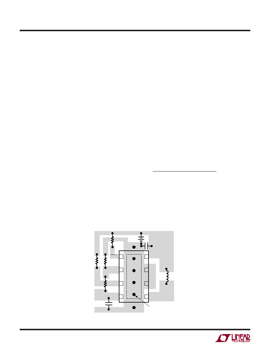
PCB LAYOUT GUIDELINES
The high speed operation of the LTC3528/LTC3528B de-
mands careful attention to board layout. A careless layout
will not produce the advertised performance. Figure 1
shows the recommended component placement. A large
ground copper area with the package backside metal pad
properly soldered will help to lower the chip temperature.
A multilayer board with a separate ground plane is ideal,
but not absolutely necessary.
COMPONENT SELECTION
Inductor Selection
The LTC3528/LTC3528B can utilize small surface mount
chip inductors due to their fast 1MHz switching frequency.
Inductor values between 2.2μH and 4.7μH are suitable for
most applications. Larger values of inductance will allow
slightly greater output current capability (and lower the
Burst Mode threshold) by reducing the inductor ripple cur-
rent. Increasing the inductance above 10μH will increase
size while providing little improvement in output current
capability.
The minimum inductance value is given by:
L
VV
V
Ripple V
IN MIN
OUT MAX
IN MIN
>
()
(
)
()
–
.
12
O
OUT MAX
μH
()
where:
Ripple = Allowable inductor current ripple (amps peak-
peak)
VIN(MIN) = Minimum input voltage
VOUT(MAX) = Maximum output voltage
SHDN
FB
PGOOD
LTC3528
VOUT
3528 F01
COUT
VIN
CIN
SGND
PGND
SW
MULTIPLE VIAS
TO GROUND PLANE
8
5
6
7
1
4
3
2
+
Figure 1. Recommended Component Placement for Single Layer Board
相关PDF资料 |
PDF描述 |
|---|---|
| LTC3528EDDB#TRM | SWITCHING REGULATOR, 1300 kHz SWITCHING FREQ-MAX, PDSO8 |
| LTC3542EDC-1#PBF | SWITCHING REGULATOR, 2700 kHz SWITCHING FREQ-MAX, PDSO6 |
| LTC3547BIDDB#TRM | 0.7 A DUAL SWITCHING CONTROLLER, 2700 kHz SWITCHING FREQ-MAX, PDSO8 |
| LTC3547BEDDB-1#PBF | 0.7 A DUAL SWITCHING CONTROLLER, 2700 kHz SWITCHING FREQ-MAX, PDSO8 |
| LTC3547BIDDB#PBF | 0.7 A DUAL SWITCHING CONTROLLER, 2700 kHz SWITCHING FREQ-MAX, PDSO8 |
相关代理商/技术参数 |
参数描述 |
|---|---|
| LTC3528BEDDB-TRPBF | 制造商:LINER 制造商全称:Linear Technology 功能描述:1A, 1MHz Synchronous Step-Up DC/DC Converters in 3mm × 2mm DFN |
| LTC3528EDDB#PBF | 制造商:Linear Technology 功能描述:DP-SWREG/Monolithic, Cut Tape 1A, 1MHz Synch Boost converter w/ Output Disconnec |
| LTC3528EDDB#TRMPBF | 功能描述:IC REG BOOST SYNC ADJ 1A 8DFN RoHS:是 类别:集成电路 (IC) >> PMIC - 稳压器 - DC DC 开关稳压器 系列:- 标准包装:250 系列:- 类型:降压(降压) 输出类型:固定 输出数:1 输出电压:1.2V 输入电压:2.05 V ~ 6 V PWM 型:电压模式 频率 - 开关:2MHz 电流 - 输出:500mA 同步整流器:是 工作温度:-40°C ~ 85°C 安装类型:表面贴装 封装/外壳:6-UFDFN 包装:带卷 (TR) 供应商设备封装:6-SON(1.45x1) 产品目录页面:1032 (CN2011-ZH PDF) 其它名称:296-25628-2 |
| LTC3528EDDB#TRPBF | 功能描述:IC REG BOOST SYNC ADJ 1A 8DFN RoHS:是 类别:集成电路 (IC) >> PMIC - 稳压器 - DC DC 开关稳压器 系列:- 标准包装:2,500 系列:- 类型:升压(升压) 输出类型:可调式 输出数:1 输出电压:1.24 V ~ 30 V 输入电压:1.5 V ~ 12 V PWM 型:电流模式,混合 频率 - 开关:600kHz 电流 - 输出:500mA 同步整流器:无 工作温度:-40°C ~ 85°C 安装类型:表面贴装 封装/外壳:8-SOIC(0.154",3.90mm 宽) 包装:带卷 (TR) 供应商设备封装:8-SOIC |
| LTC3528EDDB-2 | 制造商:LINER 制造商全称:Linear Technology 功能描述:1A, 2MHz Synchronous Step-Up DC/DC Converter in 2mm × 3mm DFN |
发布紧急采购,3分钟左右您将得到回复。