- 您现在的位置:买卖IC网 > PDF目录44991 > LTC3533EDE (LINEAR TECHNOLOGY CORP) 7 A SWITCHING REGULATOR, 2000 kHz SWITCHING FREQ-MAX, PDSO14 PDF资料下载
参数资料
| 型号: | LTC3533EDE |
| 厂商: | LINEAR TECHNOLOGY CORP |
| 元件分类: | 稳压器 |
| 英文描述: | 7 A SWITCHING REGULATOR, 2000 kHz SWITCHING FREQ-MAX, PDSO14 |
| 封装: | 4 X 3 MM, 0.75 MM HEIGHT, PLASTIC, MO-229WGED-3, DFN-14 |
| 文件页数: | 15/16页 |
| 文件大小: | 313K |
| 代理商: | LTC3533EDE |
LTC3533
8
3533f
OPERATION
Error Amplier
The error amplier is a voltage mode amplier. The loop
compensation components are congured around the
amplier (from FB to VC) to obtain stability of the converter.
For improved bandwidth, an additional RC feed-forward
network can be placed across the upper feedback divider
resistor. The voltage on the RUN/SS pin clamps the error
amplier output, VC, to provide a soft-start function.
Supply Current Limits
There are two different supply current limit circuits in the
LTC3533, working consecutively, each having internally
xed thresholds which vary inversely with VIN.
The rst circuit is a current limit amplier, sourcing cur-
rent into FB to drop the output voltage, should the peak
input current exceed 4.5A typical. This method provides a
closed loop means of clamping the input current. During
conditions where VOUT is near ground, such as during a
short circuit or startup, this threshold is cut to 750mA,
providing a fold-back feature. For this current limit feature
to be most effective, the Thevenin resistance from FB to
ground should be greater than 100k.
Should the peak input current exceed 7A typical, the second
circuit, a high speed peak current limit comparator, shuts
off PMOS switch A. The delay to output of this comparator
is typically 50ns.
Reverse Current Limit
During xed frequency operation, the LTC3533 operates in
forced continuous conduction mode. The reverse current
limit comparator monitors the inductor current from the
output through switch D. Should this negative inductor
current exceed 500mA typical, the LTC3533 shuts off
switch D.
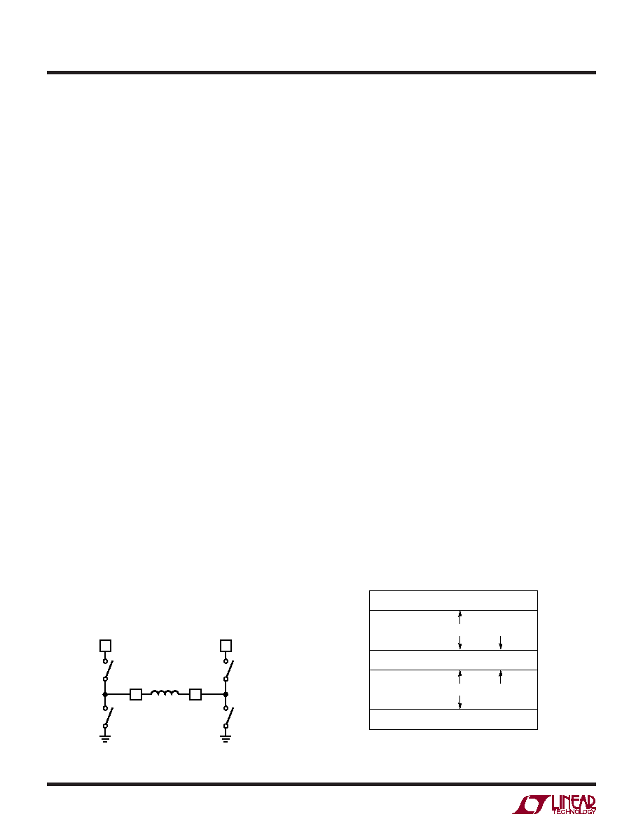
Four-Switch Control
Figure 1 shows a simplied diagram of how the four in-
ternal switches are connected to the inductor, VIN, VOUT
and GND.Figure 2 shows the regions of operation for the
LTC3533 as a function of the control voltage, VC.
Dependent on VC’s magnitude, the LTC3533 will operate
in either buck, buck/boost or boost mode. The four power
switches are properly phased so the transfer between op-
erating modes is continuous, smooth and transparent to
the user. When VIN approaches VOUT the buck/boost region
is entered, where the conduction time of the four switch
region is typically 150ns. Referring to Figures 1 and 2, the
various regions of operation will now be described.
Buck Region (VIN > VOUT)
Switch D is always on and switch C is always off during
this mode. When the control voltage, VC, is above volt-
age V1, switch A begins to switch. During the off time of
switch A, synchronous switch B turns on for the remainder
of the period. Switches A and B will alternate similar to a
typical synchronous buck regulator. As the control volt-
age increases, the duty cycle of switch A increases until
the maximum duty cycle of the converter in buck mode
reaches DMAX_BUCK, given by:
DMAX_BUCK = 100 – D4SW %
where D4SW = duty cycle % of the four switch range.
3
SW1
7
SW2
PMOS A
NMOS B
11
PVIN
PMOS D
NMOS C
3533 F01
9
PVOUT
L1
85%
DMAX
BOOST
DMIN
BOOST
DMAX
BUCK
DUTY
CYCLE
0%
V4 (
≈1.5V)
V3 (
≈1.15V)
BOOST REGION
BUCK REGION
BUCK/BOOST REGION
V2 (
≈1V)
V1 (
≈0.7V)
3533 F02
A ON, B OFF
PWM CD SWITCHES
D ON, C OFF
PWM AB SWITCHES
FOUR SWITCH PWM
CONTROL
VOLTAGE, VC
Figure 1. Simplied Diagram of Output Switches
Figure 2. Switch Control vs Control Voltage, VC
相关PDF资料 |
PDF描述 |
|---|---|
| LTC3535EDD#PBF | SWITCHING REGULATOR, PDSO12 |
| LTC3538EDCB#PBF | 0.8 A SWITCHING REGULATOR, 1200 kHz SWITCHING FREQ-MAX, PDSO8 |
| LTC3538EDCB | 0.8 A SWITCHING REGULATOR, 1200 kHz SWITCHING FREQ-MAX, PDSO8 |
| LTC3538EDCB#TR | 0.8 A SWITCHING REGULATOR, 1200 kHz SWITCHING FREQ-MAX, PDSO8 |
| LTC3541EDD-2 | 1.25 A SWITCHING REGULATOR, 2700 kHz SWITCHING FREQ-MAX, PDSO10 |
相关代理商/技术参数 |
参数描述 |
|---|---|
| LTC3533EDE#PBF | 功能描述:IC REG BUCK BOOST SYNC ADJ 14DFN RoHS:是 类别:集成电路 (IC) >> PMIC - 稳压器 - DC DC 开关稳压器 系列:- 标准包装:250 系列:- 类型:降压(降压) 输出类型:固定 输出数:1 输出电压:1.2V 输入电压:2.05 V ~ 6 V PWM 型:电压模式 频率 - 开关:2MHz 电流 - 输出:500mA 同步整流器:是 工作温度:-40°C ~ 85°C 安装类型:表面贴装 封装/外壳:6-UFDFN 包装:带卷 (TR) 供应商设备封装:6-SON(1.45x1) 产品目录页面:1032 (CN2011-ZH PDF) 其它名称:296-25628-2 |
| LTC3533EDE#PBF | 制造商:Linear Technology 功能描述:DC/DC Converter IC |
| LTC3533EDE#TRPBF | 功能描述:IC REG BUCK BOOST SYNC ADJ 14DFN RoHS:是 类别:集成电路 (IC) >> PMIC - 稳压器 - DC DC 开关稳压器 系列:- 标准包装:2,500 系列:- 类型:降压(降压) 输出类型:固定 输出数:1 输出电压:1.2V,1.5V,1.8V,2.5V 输入电压:2.7 V ~ 20 V PWM 型:- 频率 - 开关:- 电流 - 输出:50mA 同步整流器:是 工作温度:-40°C ~ 125°C 安装类型:表面贴装 封装/外壳:10-TFSOP,10-MSOP(0.118",3.00mm 宽)裸露焊盘 包装:带卷 (TR) 供应商设备封装:10-MSOP 裸露焊盘 |
| LTC3533EDEPBF | 制造商:Linear Technology 功能描述:2A 1.8-5.5V Synch Buck-Boost DC/DC DFN14 |
| LTC3534 | 制造商:LINER 制造商全称:Linear Technology 功能描述:40V, 2A Synchronous Buck-Boost DC/DC |
发布紧急采购,3分钟左右您将得到回复。