- 您现在的位置:买卖IC网 > PDF目录1830 > LTC3536IMSE#TRPBF (Linear Technology)IC REG BUCK BST SYNC ADJ 12MSOP PDF资料下载
参数资料
| 型号: | LTC3536IMSE#TRPBF |
| 厂商: | Linear Technology |
| 文件页数: | 9/28页 |
| 文件大小: | 0K |
| 描述: | IC REG BUCK BST SYNC ADJ 12MSOP |
| 标准包装: | 2,500 |
| 类型: | 降压(降压),升压(升压) |
| 输出类型: | 可调式 |
| 输出数: | 1 |
| 输出电压: | 1.8 V ~ 5.5 V |
| 输入电压: | 1.8 V ~ 5.5 V |
| PWM 型: | 电压模式,混合 |
| 频率 - 开关: | 300kHz ~ 2MHz |
| 电流 - 输出: | 1A |
| 同步整流器: | 是 |
| 工作温度: | -40°C ~ 125°C |
| 安装类型: | 表面贴装 |
| 封装/外壳: | 12-TSSOP (0.118",3.00mm 宽)裸露焊盘 |
| 包装: | 带卷 (TR) |
| 供应商设备封装: | 12-MSOP,裸露焊盘 |
第1页第2页第3页第4页第5页第6页第7页第8页当前第9页第10页第11页第12页第13页第14页第15页第16页第17页第18页第19页第20页第21页第22页第23页第24页第25页第26页第27页第28页
�� �
�
�LTC3536�
�OPERATION�
�L�
�INTRODUCTION�
�The� LTC3536� is� a� monolithic� buck-boost� converter� that�
�can� operate� with� input� and� output� voltages� from� as� low�
�as� 1.8V� to� as� high� as� 5.5V.� A� proprietary� switch� control�
�algorithm� allows� the� buck-boost� converter� to� maintain�
�output� voltage� regulation� with� input� voltages� that� are�
�above,� below� or� equal� to� the� output� voltage.� Transitions�
�between� these� operating� modes� are� seamless� and� free� of�
�transients� and� subharmonic� switching.�
�The� LTC3536� can� be� configured� to� operate� over� a� wide�
�range� of� switching� frequencies,� from� 300kHz� to� 2MHz,�
�allowing� applications� to� be� optimized� for� board� area� and�
�efficiency.� The� LTC3536� has� an� internal� fixed-frequency�
�oscillator� with� a� switching� frequency� that� is� easily� set� by�
�a� single� external� resistor.� In� noise� sensitive� applications,�
�the� converter� can� also� be� synchronized� to� an� external� clock�
�via� the� MODE/SYNC� pin.� The� operating� frequency� defaults�
�to� 1.2MHz� when� RT� is� connected� to� V� IN� eliminating� the�
�external� resistor.�
�The� LTC3536� has� been� optimized� to� reduce� input� current�
�in� shutdown� and� standby� for� applications� that� are� sensi-�
�tive� to� quiescent� current� draw,� such� as� battery-powered�
�devices.� In� Burst� Mode� operation,� the� no-load� standby�
�current� is� only� 32μA� and� in� shutdown� the� total� supply�
�current� is� reduced� to� less� than� 1μA.�
�PWM� MODE� OPERATION�
�With� the� MODE/SYNC� pin� forced� low� or� driven� by� an�
�external� clock,� the� LTC3536� operates� in� a� fixed-frequency�
�pulse-width� modulation� (PWM)� mode� using� a� voltage� mode�
�control� loop.� This� mode� of� operation� maximizes� the� output�
�current� that� can� be� delivered� by� the� converter,� reduces� out-�
�put� voltage� ripple,� and� yields� a� low� noise� fixed-frequency�
�switching� spectrum.� A� proprietary� switching� algorithm�
�provides� seamless� transitions� between� operating� modes�
�and� eliminates� discontinuities� in� the� average� inductor� cur-�
�rent,� inductor� current� ripple,� and� loop� transfer� function�
�throughout� all� regions� of� operation.� These� advantages�
�result� in� increased� efficiency,� improved� loop� stability,� and�
�lower� output� voltage� ripple� in� comparison� to� the� traditional�
�4-switch� buck-boost� converter.�
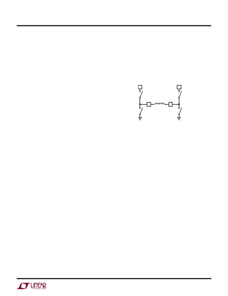
�Figure� 1� shows� the� topology� of� the� LTC3536� power� stage�
�which� is� comprised� of� two� P-channel� MOSFET� switches�
�and� two� N-channel� MOSFET� switches� and� their� associated�
�gate� drivers.� In� response� to� the� error� amplifier� output,� an�
�internal� pulse-width� modulator� generates� the� appropriate�
�switch� duty� cycles� to� maintain� regulation� of� the� output�
�voltage.�
�V� IN� V� OUT�
�PMOS� A� PMOS� D�
�SW1� SW2�
�NMOS� B� NMOS� C�
�3536� F01�
�Figure� 1.� Power� Stage� Schematic�
�When� the� input� voltage� is� significantly� greater� than� the�
�output� voltage,� the� buck-boost� converter� operates� in�
�buck� mode.� Switch� D� turns� on� continuously� and� switch�
�C� remains� off.� Switch� A� and� B� are� pulse-width� modulated�
�to� produce� the� required� duty� cycle� to� support� the� output�
�regulation� voltage.� As� the� input� voltage� decreases,� switch?A�
�remains� on� for� a� larger� portion� of� the� switching� cycle.�
�When� the� duty� cycle� reaches� approximately� 90%� the�
�switch� pair� AC� begins� turning� on� for� a� small� fraction� of� the�
�switching� period.� As� the� input� voltage� decreases� further,�
�the� AC� switch� pair� remains� on� for� longer� durations� and�
�the� duration� of� the� BD� phase� decreases� proportionally.� At�
�this� point,� switch� A� remains� on� continuously� while� switch�
�pair� CD� is� pulse-width� modulated� to� obtain� the� desired�
�output� voltage.� At� this� point,� the� converter� is� operating�
�solely� in� boost� mode.�
�Oscillator� and� Phase-Locked� Loop�
�The� LTC3536� operates� from� an� internal� oscillator� with� a�
�switching� frequency� that� can� be� configured� by� a� single�
�external� resistor� between� RT� and� ground.� Tying� RT� to� V� IN�
�sets� the� default� internal� operating� frequency� to� typically�
�1.2MHz.� If� the� RT� pin� is� driven� externally� to� a� level� higher�
�than� V� IN� ,� a� current� limiting� resistor� should� be� used.� 1M� for�
�6V� on� the� RT� pin� limits� the� current� to� 6μA.� Also,� a� Schottky�
�3536fa�
�9�
�相关PDF资料 |
PDF描述 |
|---|---|
| LTC3538EDCB#TRPBF | IC REG BUCK BOOST SYNC ADJ 8DFN |
| LTC3539EDCB-2#TRPBF | IC REG BOOST SYNC ADJ 2A 8DFN |
| LTC3542IDC#TRMPBF | IC REG BUCK SYNC ADJ 0.5A 6DFN |
| LTC3543EDCB#TRPBF | IC REG BUCK SYNC ADJ 0.6A 8DFN |
| LTC3544BEUD#TRPBF | IC REG BUCK SYNC ADJ QUAD 16QFN |
相关代理商/技术参数 |
参数描述 |
|---|---|
| LTC3537 | 制造商:LINER 制造商全称:Linear Technology 功能描述:2.2 MHz, 600mA Synchronous Step-Up DC/DC Converter and 100mA LDO |
| LTC3537EUD#PBF | 功能描述:IC REG DL BST/LINEAR SYNC 16-QFN RoHS:是 类别:集成电路 (IC) >> PMIC - 稳压器 - 线性 + 切换式 系列:- 标准包装:2,500 系列:- 拓扑:降压(降压)同步(3),线性(LDO)(2) 功能:任何功能 输出数:5 频率 - 开关:300kHz 电压/电流 - 输出 1:控制器 电压/电流 - 输出 2:控制器 电压/电流 - 输出 3:控制器 带 LED 驱动器:无 带监控器:无 带序列发生器:是 电源电压:5.6 V ~ 24 V 工作温度:-40°C ~ 85°C 安装类型:* 封装/外壳:* 供应商设备封装:* 包装:* |
| LTC3537EUD#TRPBF | 功能描述:IC REG DL BST/LINEAR SYNC 16-QFN RoHS:是 类别:集成电路 (IC) >> PMIC - 稳压器 - 线性 + 切换式 系列:- 标准包装:2,500 系列:- 拓扑:降压(降压)同步(3),线性(LDO)(2) 功能:任何功能 输出数:5 频率 - 开关:300kHz 电压/电流 - 输出 1:控制器 电压/电流 - 输出 2:控制器 电压/电流 - 输出 3:控制器 带 LED 驱动器:无 带监控器:无 带序列发生器:是 电源电压:5.6 V ~ 24 V 工作温度:-40°C ~ 85°C 安装类型:* 封装/外壳:* 供应商设备封装:* 包装:* |
| LTC3537EUD-PBF | 制造商:LINER 制造商全称:Linear Technology 功能描述:2.2 MHz, 600mA Synchronous Step-Up DC/DC Converter and 100mA LDO |
| LTC3537EUD-TRPBF | 制造商:LINER 制造商全称:Linear Technology 功能描述:2.2 MHz, 600mA Synchronous Step-Up DC/DC Converter and 100mA LDO |
发布紧急采购,3分钟左右您将得到回复。