- 您现在的位置:买卖IC网 > PDF目录98003 > LTC3542IS6#PBF (LINEAR TECHNOLOGY CORP) SWITCHING REGULATOR, 2700 kHz SWITCHING FREQ-MAX, PDSO6 PDF资料下载
参数资料
| 型号: | LTC3542IS6#PBF |
| 厂商: | LINEAR TECHNOLOGY CORP |
| 元件分类: | 稳压器 |
| 英文描述: | SWITCHING REGULATOR, 2700 kHz SWITCHING FREQ-MAX, PDSO6 |
| 封装: | LEAD FREE, PLASTIC, MO-193, TSOT-23, 6 PIN |
| 文件页数: | 2/16页 |
| 文件大小: | 211K |
| 代理商: | LTC3542IS6#PBF |
LTC3542
10
3542fa
Output Voltage Programming
The output voltage is set by a resistive divider according
to the following formula:
VV
R
OUT =+
06
1
2
1
.
To improve the frequency response, a feed-forward capaci-
tor, CF, may also be used. Great care should be taken to
route the VFB line away from noise sources, such as the
inductor or the SW line.
Mode Selection and Frequency Synchronization
The MODE/SYNC pin is a multipurpose pin that provides
mode selection and frequency synchronization. Connect-
ing this pin to GND enables Burst Mode operation, which
provides the best low current efciency at the cost of a
higher output voltage ripple. Connecting this pin to VIN
selects pulse skip mode operation, which provides the
lowest output ripple at the cost of low current efciency.
The LTC3542 can also be synchronized to an external clock
signal with range from 1MHz to 3MHz by the MODE/SYNC
pin. During synchronization, the mode is set to pulse skip
and the top switch turn-on is synchronized to the falling
edge of the external clock.
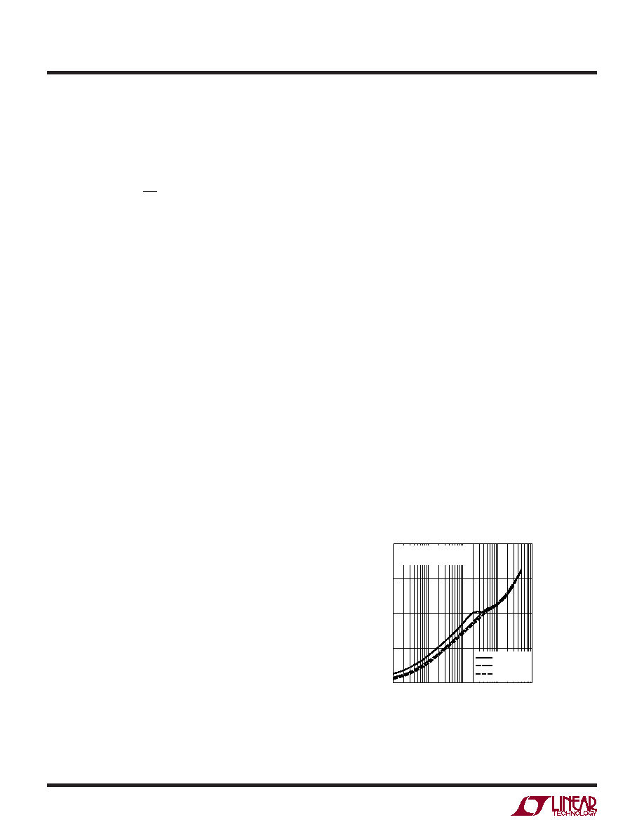
Efciency Considerations
The efciency of a switching regulator is equal to the output
power divided by the input power times 100%. It is often
useful to analyze individual losses to determine what is
limiting the efciency and which change would produce
the most improvement. Efciency can be expressed as:
Efciency = 100% – (L1 + L2 + L3 + ...)
where L1, L2, etc. are the individual losses as a percent-
age of input power.
Although all dissipative elements in the circuit produce
losses, three main sources usually account for most of
the losses in LTC3542 circuits: 1) VIN quiescent current,
2) I2R loss and 3) switching loss. VIN quiescent current
loss dominates the power loss at very low load currents,
whereas the other two dominate at medium to high load
currents. In a typical efciency plot, the efciency curve
at very low load currents can be misleading since the
actual power loss is of no consequence as illustrated in
Figure 2.
1) The VIN quiescent current is the DC supply current given
in the Electrical Characteristics which excludes MOSFET
charging current. VIN current results in a small (<0.1%)
loss that increases with VIN, even at no load.
2) I2R losses are calculated from the DC resistances of
the internal switches, RSW, and external inductor, RL. In
continuous mode, the average output current ows through
inductor L, but is “chopped” between the internal top and
bottom switches. Thus, the series resistance looking into
the SW pin is a function of both top and bottom MOSFET
RDS(ON) and the duty cycle (D) as follows:
RSW = (RDS(ON)TOP)(D) + (RDS(ON)BOT)(1 – D)
The RDS(ON) for both the top and bottom MOSFETs can
be obtained from the Typical Performance Characteristics
curves. Thus, to obtain I2R losses:
I2R losses = IOUT2(RSW + RL)
Figure 2. Power Loss vs Load Current
OUTPUT CURRENT (mA)
1
POWER
LOSS
(mW)
10
100
1000
0.1
10
100
1000
3542 F02
0.1
1
VOUT = 2.5V
VOUT = 1.8V
VOUT = 1.2V
VIN = 3.6V
Burst Mode OPERATION
APPLICATIONS INFORMATION
相关PDF资料 |
PDF描述 |
|---|---|
| LTC3559EUD | 1.05 A BATTERY CHARGE CONTROLLER, 2590 kHz SWITCHING FREQ-MAX, PQCC16 |
| LTC3586EUFE#PBF | 3 A BATTERY CHARGE CONTROLLER, 2700 kHz SWITCHING FREQ-MAX, PQCC38 |
| LTC3586EUFE-1#PBF | BATTERY CHARGE CONTROLLER, PQCC38 |
| LTC3586EUFE-1#TRPBF | BATTERY CHARGE CONTROLLER, PQCC38 |
| LTC3672BEDC-1#PBF | 1.1 A SWITCHING REGULATOR, 2700 kHz SWITCHING FREQ-MAX, PDSO8 |
相关代理商/技术参数 |
参数描述 |
|---|---|
| LTC3542IS6-TRPBF | 制造商:LINER 制造商全称:Linear Technology 功能描述:500mA, 2.25MHz Synchronous Step-Down DC/DC Converter |
| LTC3543 | 制造商:LINER 制造商全称:Linear Technology 功能描述:600mA Synchronous Step Down Buck Regulator with PLL, Soft-Start and Spread Spectrum |
| LTC3543EDCB | 制造商:LINER 制造商全称:Linear Technology 功能描述:600mA Synchronous Step Down Buck Regulator with PLL, Soft-Start and Spread Spectrum |
| LTC3543EDCB#PBF | 制造商:Linear Technology 功能描述:REG STEP DOWN 0.6A SMD DFN-6 制造商:Linear Technology 功能描述:REG, STEP DOWN, 0.6A, SMD, DFN-6 |
| LTC3543EDCB#TRMPBF | 功能描述:IC REG BUCK SYNC ADJ 0.6A 8DFN RoHS:是 类别:集成电路 (IC) >> PMIC - 稳压器 - DC DC 开关稳压器 系列:- 标准包装:2,500 系列:- 类型:升压(升压) 输出类型:可调式 输出数:1 输出电压:1.24 V ~ 30 V 输入电压:1.5 V ~ 12 V PWM 型:电流模式,混合 频率 - 开关:600kHz 电流 - 输出:500mA 同步整流器:无 工作温度:-40°C ~ 85°C 安装类型:表面贴装 封装/外壳:8-SOIC(0.154",3.90mm 宽) 包装:带卷 (TR) 供应商设备封装:8-SOIC |
发布紧急采购,3分钟左右您将得到回复。