- 您现在的位置:买卖IC网 > PDF目录44991 > LTC3543EDCB#PBF (LINEAR TECHNOLOGY CORP) 1.3 A SWITCHING REGULATOR, 2250 kHz SWITCHING FREQ-MAX, PDSO6 PDF资料下载
参数资料
| 型号: | LTC3543EDCB#PBF |
| 厂商: | LINEAR TECHNOLOGY CORP |
| 元件分类: | 稳压器 |
| 英文描述: | 1.3 A SWITCHING REGULATOR, 2250 kHz SWITCHING FREQ-MAX, PDSO6 |
| 封装: | 2 X 3 MM, 0.75 MM HEIGHT, LEAD FREE, PLASTIC, MO-229, DFN-6 |
| 文件页数: | 7/20页 |
| 文件大小: | 329K |
| 代理商: | LTC3543EDCB#PBF |
LTC3543
15
3543fa
Checking Transient Response
The regulator loop response can be checked by looking
at the load transient response. Switching regulators take
several cycles to respond to a step in load current. When
a load step occurs, VOUT immediately shifts by an amount
equal to (
ΔILOAD ESR), where ESR is the effective series
resistance of COUT.
ΔILOAD also begins to charge or dis-
charge COUT, which generates a feedback error signal.
The regulator loop then acts to return VOUT to its steady
state value. During this recovery time, VOUT can be moni-
tored for overshoot or ringing that would indicate a stability
problem. For a detailed explanation of the switching control
loop theory, see Application Note 76.
A second, more severe transient is caused by switching
in loads with large (>1μF) supply bypass capacitors. The
discharged bypass capacitors are effectively put in paral-
lel with COUT, causing a rapid drop in VOUT. No regulator
can deliver enough current to prevent this problem if the
load switch resistance is low and it is driven quickly. The
only solution is to limit the rise time of the switch drive
so that the load rise time is limited to approximately
25 CLOAD. Thus, a 10μF capacitor charging to 3.3V would
require a 250μs rise time, limiting the charging current
to about 130mA.
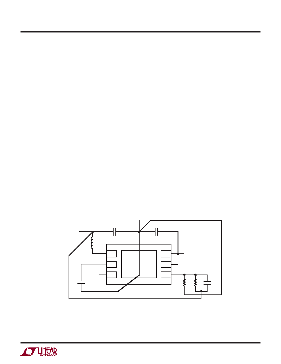
PC Board Layout Checklist
When laying out the printed circuit board, the follow-
ing checklist should be used to ensure proper opera-
tion of the LTC3543. These items are also illustrated
graphically in Figures 5 and 6. Check the following in
your layout:
1. The power traces, consisting of the GND trace, the SW
trace, and the VIN trace should be kept short, direct
and wide.
2. Does the VFB pin connect directly to the feedback volt-
age reference? Ensure that there is no load current
running from the feedback reference voltage and the
VFB pin.
3. Does the (+) plate of CIN connect to VIN as closely as
possible? This capacitor provides the AC current to the
internal power MOSFETs.
4. Keep the switching node, SW, away from the sensitive
VFB node.
5. Keep the (–) plates of CIN and COUT as close as pos-
sible.
APPLICATIONS INFORMATION
4
5
6
3
2
1
R1
R2
SW
VIN
VFB
MODE
RUN
CFWD
CIN
C1
GND
L
VIN
CAP
VOUT
COUT
3543 F05
+–
+
–
+
–
+–
Figure 5. LTC3543 Layout Diagram
相关PDF资料 |
PDF描述 |
|---|---|
| LTC3543EDCB#TRM | 1.3 A SWITCHING REGULATOR, 2250 kHz SWITCHING FREQ-MAX, PDSO6 |
| LTC3543EDCB | 1.3 A SWITCHING REGULATOR, 2250 kHz SWITCHING FREQ-MAX, PDSO6 |
| LTC3544BEUD#TR | 0.8 A SWITCHING REGULATOR, 2700 kHz SWITCHING FREQ-MAX, PQCC16 |
| LTC3544EUD | 0.8 A SWITCHING REGULATOR, 2700 kHz SWITCHING FREQ-MAX, PQCC16 |
| LTC3547BEDDB | 0.7 A DUAL SWITCHING CONTROLLER, 2700 kHz SWITCHING FREQ-MAX, PDSO8 |
相关代理商/技术参数 |
参数描述 |
|---|---|
| LTC3544 | 制造商:LINER 制造商全称:Linear Technology 功能描述:Quad Synchronous Step-Down Regulator: 2.25MHz, 300mA, 200mA, 200mA, 100mA |
| LTC3544B | 制造商:LINER 制造商全称:Linear Technology 功能描述:Quad Synchronous Step-Down Regulator: 2.25MHz, 300mA, 200mA, 200mA, 100mA |
| LTC3544BEUD | 制造商:LINER 制造商全称:Linear Technology 功能描述:Quad Synchronous Step-Down Regulator: 2.25MHz, 300mA, 200mA, 200mA, 100mA |
| LTC3544BEUD#PBF | 功能描述:IC REG BUCK SYNC ADJ QUAD 16QFN RoHS:是 类别:集成电路 (IC) >> PMIC - 稳压器 - DC DC 开关稳压器 系列:- 标准包装:250 系列:- 类型:降压(降压) 输出类型:固定 输出数:1 输出电压:1.2V 输入电压:2.05 V ~ 6 V PWM 型:电压模式 频率 - 开关:2MHz 电流 - 输出:500mA 同步整流器:是 工作温度:-40°C ~ 85°C 安装类型:表面贴装 封装/外壳:6-UFDFN 包装:带卷 (TR) 供应商设备封装:6-SON(1.45x1) 产品目录页面:1032 (CN2011-ZH PDF) 其它名称:296-25628-2 |
| LTC3544BEUD#TRPBF | 功能描述:IC REG BUCK SYNC ADJ QUAD 16QFN RoHS:是 类别:集成电路 (IC) >> PMIC - 稳压器 - DC DC 开关稳压器 系列:- 标准包装:2,500 系列:- 类型:降压(降压) 输出类型:固定 输出数:1 输出电压:1.2V,1.5V,1.8V,2.5V 输入电压:2.7 V ~ 20 V PWM 型:- 频率 - 开关:- 电流 - 输出:50mA 同步整流器:是 工作温度:-40°C ~ 125°C 安装类型:表面贴装 封装/外壳:10-TFSOP,10-MSOP(0.118",3.00mm 宽)裸露焊盘 包装:带卷 (TR) 供应商设备封装:10-MSOP 裸露焊盘 |
发布紧急采购,3分钟左右您将得到回复。