- 您现在的位置:买卖IC网 > PDF目录44991 > LTC3563EDC (LINEAR TECHNOLOGY CORP) 1.75 A SWITCHING REGULATOR, 2700 kHz SWITCHING FREQ-MAX, PDSO6 PDF资料下载
参数资料
| 型号: | LTC3563EDC |
| 厂商: | LINEAR TECHNOLOGY CORP |
| 元件分类: | 稳压器 |
| 英文描述: | 1.75 A SWITCHING REGULATOR, 2700 kHz SWITCHING FREQ-MAX, PDSO6 |
| 封装: | 2 X 2 MM, PLASTIC, MO-229WCCD-2, DFN-6 |
| 文件页数: | 3/16页 |
| 文件大小: | 276K |
| 代理商: | LTC3563EDC |
LTC3563
11
3563f
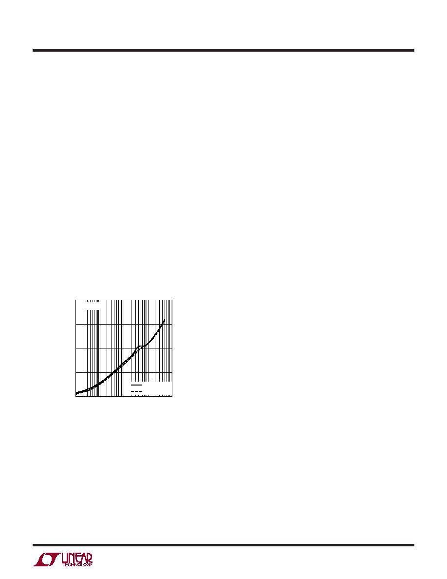
Efciency Considerations
The efciency of a switching regulator is equal to the output
power divided by the input power times 100%. It is often
useful to analyze individual losses to determine what is
limiting the efciency and which change would produce
the most improvement. Efciency can be expressed as:
Efciency = 100% – (L1 + L2 + L3 + ...)
where L1, L2, etc. are the individual losses as a percent-
age of input power.
Although all dissipative elements in the circuit produce
losses, three main sources usually account for most of
the losses in LTC3563 circuits: 1) VIN quiescent current,
2) I2R loss and 3) switching loss. VIN quiescent current
loss dominates the power loss at very low load currents,
whereas the other two dominate at medium to high load
currents. In a typical efciency plot, the efciency curve
at very low load currents can be misleading since the
actual power loss is of no consequence as illustrated in
Figure 2.
1) The VIN quiescent current is the DC supply current given
in the Electrical Characteristics which excludes MOSFET
charging current. VIN current results in a small (<0.1%)
loss that increases with VIN, even at no load.
2) I2R losses are calculated from the DC resistances of
the internal switches, RSW, and external inductor, RL. In
continuous mode, the average output current ows through
inductor L, but is “chopped” between the internal top and
bottom switches. Thus, the series resistance looking into
the SW pin is a function of both top and bottom MOSFET
RDS(ON) and the duty cycle (D) as follows:
RSW = (RDS(ON)TOP)(D) + (RDS(ON)BOT)(1 – D)
The RDS(ON) for both the top and bottom MOSFETs can
be obtained from the Typical Performance Characteristics
curves. Thus, to obtain I2R losses:
I2R losses = IOUT
2(RSW + RL)
3) The switching current is MOSFET gate charging current,
that results from switching the gate capacitance of the
power MOSFETs. Each time a MOSFET gate is switched
from low to high to low again, a packet of charge dQ moves
from VIN to ground. The resulting dQ/dt is a current out of
VIN that is typically much larger than the DC bias current.
In continuous mode, IGATECHG = fO(QT + QB), where QT
and QB are the gate charges of the internal top and bottom
MOSFET switches. The gate charge losses are proportional
to VIN and thus their effects will be more pronounced at
higher supply voltages.
Other “hidden” losses such as copper trace and internal
battery resistances can account for additional efciency
degradations in portable systems. The internal battery
and fuse resistance losses can be minimized by making
sure that CIN has adequate charge storage and very low
ESR at the switching frequency. Other losses include
diode conduction losses during dead-time and inductor
core losses generally account for less than 2% total ad-
ditional loss.
APPLICATIO S I FOR ATIO
WU
UU
Figure 2. Power Loss vs Load Current
OUTPUT CURRENT (mA)
1
POWER
LOSS
(mW)
10
100
1000
0.1
10
100
1000
3563 F02
0.1
1
VOUT = 1.87V
VOUT = 1.28V
VIN = 3.6V
相关PDF资料 |
PDF描述 |
|---|---|
| LTC3568EDD#TR | 4 A SWITCHING REGULATOR, 4000 kHz SWITCHING FREQ-MAX, PDSO10 |
| LTC3568IDD | 4 A SWITCHING REGULATOR, 4000 kHz SWITCHING FREQ-MAX, PDSO10 |
| LTC3568IDD#TR | 4 A SWITCHING REGULATOR, 4000 kHz SWITCHING FREQ-MAX, PDSO10 |
| LTC3569IFE#PBF | 2.5 A SWITCHING REGULATOR, 3000 kHz SWITCHING FREQ-MAX, PDSO16 |
| LTC3569IUD#PBF | 2.5 A SWITCHING REGULATOR, 3000 kHz SWITCHING FREQ-MAX, PQCC20 |
相关代理商/技术参数 |
参数描述 |
|---|---|
| LTC3563EDC#TRMPBF | 功能描述:IC REG BUCK SYNC 0.5A 6DFN RoHS:是 类别:集成电路 (IC) >> PMIC - 稳压器 - DC DC 开关稳压器 系列:- 标准包装:500 系列:- 类型:切换式电容器(充电泵),反相 输出类型:固定 输出数:1 输出电压:-3V 输入电压:2.3 V ~ 5.5 V PWM 型:Burst Mode? 频率 - 开关:900kHz 电流 - 输出:100mA 同步整流器:无 工作温度:-40°C ~ 85°C 安装类型:表面贴装 封装/外壳:SOT-23-6 细型,TSOT-23-6 包装:带卷 (TR) 供应商设备封装:TSOT-23-6 其它名称:LTC1983ES6-3#TRMTR |
| LTC3563EDC#TRPBF | 功能描述:IC REG BUCK SYNC 0.5A 6DFN RoHS:是 类别:集成电路 (IC) >> PMIC - 稳压器 - DC DC 开关稳压器 系列:- 标准包装:500 系列:- 类型:切换式电容器(充电泵),反相 输出类型:固定 输出数:1 输出电压:-3V 输入电压:2.3 V ~ 5.5 V PWM 型:Burst Mode? 频率 - 开关:900kHz 电流 - 输出:100mA 同步整流器:无 工作温度:-40°C ~ 85°C 安装类型:表面贴装 封装/外壳:SOT-23-6 细型,TSOT-23-6 包装:带卷 (TR) 供应商设备封装:TSOT-23-6 其它名称:LTC1983ES6-3#TRMTR |
| LTC3564 | 制造商:LINER 制造商全称:Linear Technology 功能描述:2.25MHz, 1.25A Synchronous Step-Down Regulator |
| LTC3564EDCB#PBF | 制造商:Linear Technology 功能描述:VOLTAGE REGULATOR BUCK 2.25MHZ 1.25A 制造商:Linear Technology 功能描述:VOLTAGE REGULATOR, BUCK, 2.25MHZ, 1.25A, 制造商:Linear Technology 功能描述:VOLTAGE REGULATOR, BUCK, 2.25MHZ, 1.25A, DFN-6, Primary Input Voltage:5.5V, No. of Outputs:1, Output Current:1.25A, No. of Pins:6, Operating Temperature Min:-40C, Operating Temperature Max:125C, MSL:MSL 1 - Unlimited , RoHS Compliant: Yes 制造商:Linear Technology 功能描述:DP-SWREG/Monolithic, Cut Tape 2.25MHz, 1.2A Synchronous Step-Down Regulator in T |
| LTC3564EDCB#TRMPBF | 功能描述:IC REG BUCK SYNC ADJ 1.25A 6DFN RoHS:是 类别:集成电路 (IC) >> PMIC - 稳压器 - DC DC 开关稳压器 系列:- 标准包装:250 系列:- 类型:降压(降压) 输出类型:固定 输出数:1 输出电压:1.2V 输入电压:2.05 V ~ 6 V PWM 型:电压模式 频率 - 开关:2MHz 电流 - 输出:500mA 同步整流器:是 工作温度:-40°C ~ 85°C 安装类型:表面贴装 封装/外壳:6-UFDFN 包装:带卷 (TR) 供应商设备封装:6-SON(1.45x1) 产品目录页面:1032 (CN2011-ZH PDF) 其它名称:296-25628-2 |
发布紧急采购,3分钟左右您将得到回复。