- 您现在的位置:买卖IC网 > PDF目录14017 > LTC3568EDD#TRPBF (Linear Technology)IC REG BUCK SYNC ADJ 1.8A 10DFN PDF资料下载
参数资料
| 型号: | LTC3568EDD#TRPBF |
| 厂商: | Linear Technology |
| 文件页数: | 14/18页 |
| 文件大小: | 0K |
| 描述: | IC REG BUCK SYNC ADJ 1.8A 10DFN |
| 标准包装: | 2,500 |
| 类型: | 降压(降压) |
| 输出类型: | 可调式 |
| 输出数: | 1 |
| 输出电压: | 0.8 V ~ 5 V |
| 输入电压: | 2.5 V ~ 5.5 V |
| PWM 型: | 电流模式,混合 |
| 频率 - 开关: | 最高 4MHz |
| 电流 - 输出: | 1.8A |
| 同步整流器: | 是 |
| 工作温度: | -40°C ~ 125°C |
| 安装类型: | 表面贴装 |
| 封装/外壳: | 10-WFDFN 裸露焊盘 |
| 包装: | 带卷 (TR) |
| 供应商设备封装: | 10-DFN(3x3) |
�� �
�
�LTC3568�
�APPLICATIONS� INFORMATION�
�R� T� =� 9� .� 78� ?� 10� 11� (� 1� MHz� )�
�=� 323� .� 8� k�
�L� =�
�?� ?� 1� ?�
�=� 1� .� 7� μ� H�
�Design Example�
�As� a� design� example,� consider� using� the� LTC3568� in� a� typical�
�application� with� V� IN� =� 5V.� The� load� requires� a� maximum�
�of� 1.8A� in� active� mode� and� 10mA� in� standby� mode.� The�
�output� voltage� is� V� OUT� =� 2.5V.� Since� the� load� still� needs�
�power� in� standby,� Burst� Mode� operation� is� selected� for�
�good� low� load� efficiency.�
�First,� calculate� the� timing� resistor:�
�?� 1� .� 08�
�Use� a� standard� value� of� 324k.� Next,� calculate� the� inductor�
�value� for� about� 40%� ripple� current� at� maximum� V� IN� :�
�2� .� 5� V� ?� 2� .� 5� V� ?�
�?�
�1� MHz� ?� 720� mA� ?� 5� V� ?�
�Choosing� the� closest� inductor� from� a� vendor� of� 2μH,�
�results� in� a� maximum� ripple� current� of:�
�The� closest� standard� value� is� 22μF� plus� 10μF.� Since� the�
�supply’s� output� impedance� is� very� low,� C� IN� is� typically� a�
�22μF.� In� noisy� environments,� decoupling� SV� IN� from� PV� IN�
�with� an� R6/C8� filter� of� 1� Ω� /0.1μF� may� help,� but� is� typically�
�not� needed.�
�The� output� voltage� can� now� be� programmed� by� choosing�
�the� values� of� R1� and� R2.� To� maintain� high� efficiency,� the�
�current� in� these� resistors� should� be� kept� small.� Choosing�
�2μA� with� the� 0.8V� feedback� voltage� makes� R1~400k.� A�
�close� standard� 1%� resistor� is� 412k� and� R2� is� then� 887k.�
�The� compensation� should� be� optimized� for� these� compo-�
�nents� by� examining� the� load� step� response� but� a� good� place�
�to� start� for� the� LTC3568� is� with� a� 13k� Ω� and� 1000pF� filter.�
�The� output� capacitor� may� need� to� be� increased� depending�
�on� the� actual� undershoot� during� a� load� step.�
�The� PGOOD� pin� is� a� common� drain� output� and� requires�
�a� pull-up� resistor.� A� 100k� resistor� is� used� for� adequate�
�speed.�
�?� ?� 1� ?�
�Δ� I� L� =�
�2� .� 5� V� ?�
�1� MHz� ?� 2� μ� ?�
�2� .� 5� V� ?�
�5� V� ?� ?�
�=� 625� mA�
�Figure� 1� shows� the� complete� schematic� for� this� design�
�example.�
�C� OUT� ≈� 2� .� 5�
�=� 36� μ� F�
�Forcostreasons,aceramiccapacitorwillbeused.C� OUT�
�selection� is� then� based� on� load� step� droop� instead� of� ESR�
�requirements.� For� a� 5%� output� droop:�
�1� .� 8� A�
�1� MHz� ?� (� 5� %� ?� 2� .� 5� V� )�
�C� IN�
�V� IN�
�Board Layout Considerations�
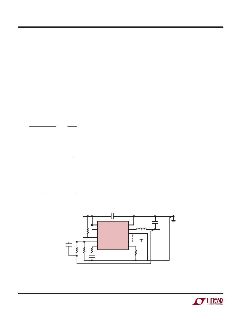
�When� laying� out� the� printed� circuit� board,� the� following�
�checklist� should� be� used� to� ensure� proper� operation� of�
�the� LTC3568.� These� items� are� also� illustrated� graphically�
�in� the� layout� diagram� of� Figure� 6.� Check� the� following� in�
�your� layout:�
�R5�
�PV� IN�
�SV� IN�
�LTC3568�
�PGND�
�SW�
�SGND�
�L1�
�C� OUT�
�V� OUT�
�PGOOD�
�PGOOD�
�V� IN�
�C4�
�R2�
�R1�
�R3�
�V� FB�
�I� TH�
�SYNC/MODE�
�SHDN/R� T�
�PS�
�BM�
�R� T�
�C3�
�3568� F06�
�BOLD� LINES� INDICATE� HIGH� CURRENT� PATHS�
�Figure 6. LTC3568 Layout Diagram (See Board Layout Checklist)�
�3568fa�
� �
�相关PDF资料 |
PDF描述 |
|---|---|
| HM53-10111HLF | HIGH POWER LOW COST INDUCTORS |
| MAX6718AUKTZD6+T | IC SUPERVISOR MPU SOT23-5 |
| GEM15DTMT-S273 | CONN EDGECARD 30POS R/A .156 SLD |
| MAX6717AUKSFD5+T | IC SUPERVISOR MPU SOT23-5 |
| ESM06DTBT-S664 | CONN EDGECARD 12POS R/A .156 |
相关代理商/技术参数 |
参数描述 |
|---|---|
| LTC3568IDD#PBF | 功能描述:IC REG BUCK SYNC ADJ 1.8A 10DFN RoHS:是 类别:集成电路 (IC) >> PMIC - 稳压器 - DC DC 开关稳压器 系列:- 标准包装:2,500 系列:- 类型:降压(降压) 输出类型:固定 输出数:1 输出电压:1.2V,1.5V,1.8V,2.5V 输入电压:2.7 V ~ 20 V PWM 型:- 频率 - 开关:- 电流 - 输出:50mA 同步整流器:是 工作温度:-40°C ~ 125°C 安装类型:表面贴装 封装/外壳:10-TFSOP,10-MSOP(0.118",3.00mm 宽)裸露焊盘 包装:带卷 (TR) 供应商设备封装:10-MSOP 裸露焊盘 |
| LTC3568IDD#PBF | 制造商:Linear Technology 功能描述:DP-SWREG/Monolithic 4MHz 1.8A Synch St 制造商:Linear Technology 功能描述:DP-SWREG/Monolithic, 4MHz, 1.8A Synch St |
| LTC3568IDD#TRPBF | 功能描述:IC REG BUCK SYNC ADJ 1.8A 10DFN RoHS:是 类别:集成电路 (IC) >> PMIC - 稳压器 - DC DC 开关稳压器 系列:- 标准包装:2,500 系列:- 类型:降压(降压) 输出类型:固定 输出数:1 输出电压:1.2V,1.5V,1.8V,2.5V 输入电压:2.7 V ~ 20 V PWM 型:- 频率 - 开关:- 电流 - 输出:50mA 同步整流器:是 工作温度:-40°C ~ 125°C 安装类型:表面贴装 封装/外壳:10-TFSOP,10-MSOP(0.118",3.00mm 宽)裸露焊盘 包装:带卷 (TR) 供应商设备封装:10-MSOP 裸露焊盘 |
| LTC3569 | 制造商:LINER 制造商全称:Linear Technology 功能描述:7-Channel Confi gurable High Power PMIC |
| LTC3569EFE | 制造商:Linear Technology 功能描述:DC/DC Converter Chip |
发布紧急采购,3分钟左右您将得到回复。