- 您现在的位置:买卖IC网 > PDF目录13932 > LTC3569IUD#PBF (Linear Technology)IC REG BUCK SYNC ADJ TRPL 20QFN PDF资料下载
参数资料
| 型号: | LTC3569IUD#PBF |
| 厂商: | Linear Technology |
| 文件页数: | 10/26页 |
| 文件大小: | 0K |
| 描述: | IC REG BUCK SYNC ADJ TRPL 20QFN |
| 标准包装: | 91 |
| 类型: | 降压(降压) |
| 输出类型: | 可调式 |
| 输出数: | 3 |
| 输出电压: | 0.43 V ~ 5.5 V |
| 输入电压: | 2.5 V ~ 5.5 V |
| PWM 型: | 电流模式,混合 |
| 频率 - 开关: | 2.25MHz,1MHz ~ 3MHz |
| 电流 - 输出: | 600mA,1.2A |
| 同步整流器: | 是 |
| 工作温度: | -40°C ~ 125°C |
| 安装类型: | 表面贴装 |
| 封装/外壳: | 20-WFQFN 裸露焊盘 |
| 包装: | 管件 |
| 供应商设备封装: | 20-QFN 裸露焊盘(3x3) |
�� �
�
�LTC3569�
�OPERATION�
�Introduction�
�The� LTC3569� contains� three� constant-frequency,� current�
�mode� buck� DC/DC� regulators.� Both� the� P-channel� and�
�synchronous� rectifier� (N-channel)� switches� are� internal�
�to� each� buck.� The� operating� frequency� is� determined� by�
�the� value� of� the� R� T� resistor,� or� is� fixed� to� 2.25MHz� by� pull-�
�ing� the� R� T� pin� to� SV� IN� ,� or� is� synchronized� to� an� external�
�oscillator� tied� to� the� MODE� pin.� Users� may� select� pulse-�
�skipping� or� Burst� Mode� operation� to� trade� off� output� ripple�
�for� efficiency.� Independent� programmable� reference� levels�
�allow� the� LTC3569� to� suit� a� variety� of� applications.�
�The� LTC3569� offers� different� power� levels,� a� single� 1.2A�
�buck� as� well� as� two� 600mA� bucks.� These� three� bucks�
�may� be� configured� in� different� parallel� configurations,�
�for� versatile� high� current� operation.� The� power� stage� of�
�buck� 2� can� be� configured� as� a� slave� to� buck� 1,� by� pulling�
�FB2� to� SV� IN� .� The� power� stage� of� buck� 3,� can� be� configured�
�to� be� a� slave� to� buck� 2,� by� pulling� the� FB3� pin� to� SV� IN� .� To�
�enable� the� slave� power� stage,� pull� the� respective� EN� pin�
�high.� However� if� the� master� is� disabled,� the� slave� power�
�stage� is� Hi-Z.�
�Each� of� the� buck� regulators� supports� 100%� duty� cycle�
�operation� (low� dropout� mode)� when� their� input� voltage�
�drops� very� close� to� their� output� voltage.� The� switching�
�regulators� also� include� soft-start� to� limit� inrush� current�
�when� powering� on,� and� short-circuit� current� protection.�
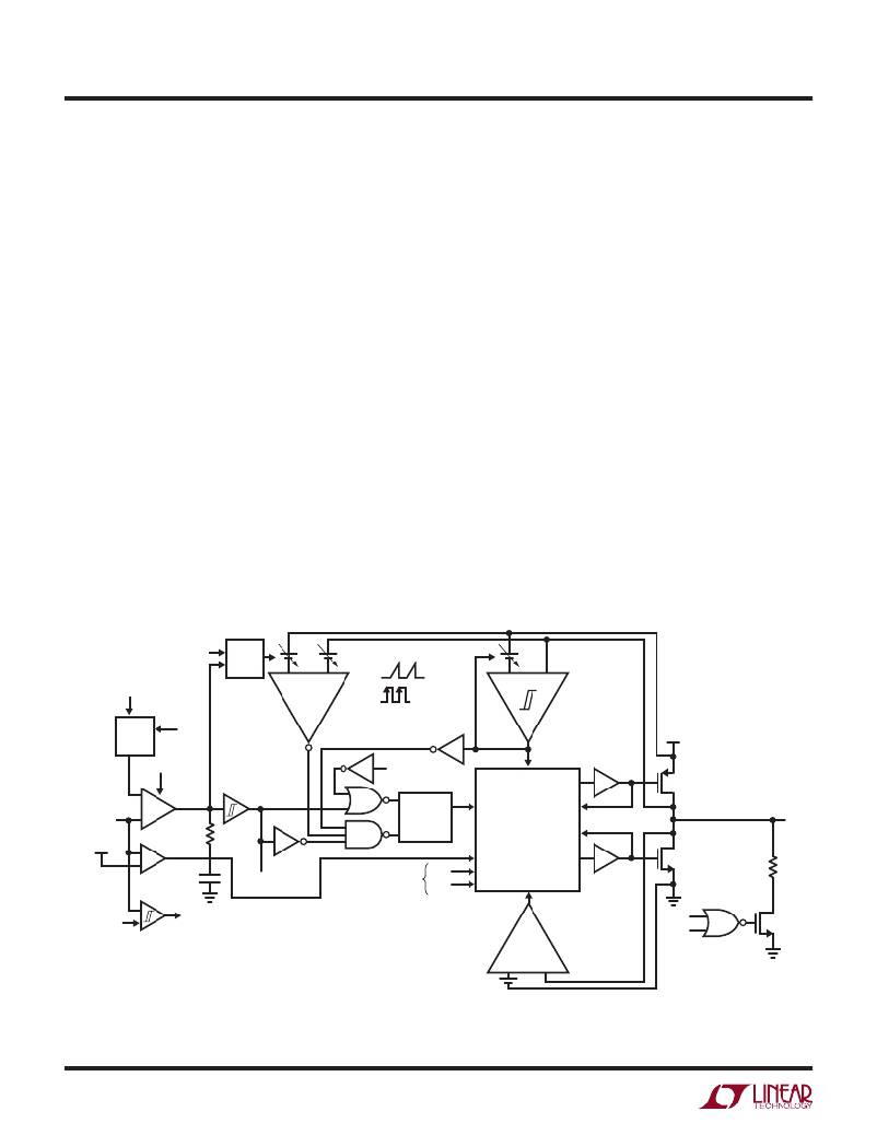
�Main� Control� Loop�
�During� normal� operation,� the� top� power� switch� (P-chan-�
�nel� MOSFET)� is� turned� on� at� the� beginning� of� a� clock�
�cycle.� The� P-channel� current� ramps� up� as� the� inductor�
�charges.� The� peak� inductor� current� is� controlled� by� the�
�internally� compensated� error� amplifier� output,� I� TH� .� The�
�current� comparator� (PCOMP)� turns� off� the� P-channel� and�
�turns� on� the� N-channel� synchronous� rectifier� when� the�
�inductor� current� reaches� the� I� TH� level� minus� the� offset� of�
�the� slope� compensation� ramp.� The� energy� stored� in� the�
�inductor� continues� to� flow� through� the� bottom� switch�
�(N-channel)� and� into� the� load� until� either� the� inductor�
�current� approaches� zero,� or� the� next� clock� cycle� begins.�
�If� the� inductor� current� approaches� zero� the� N� comparator�
�V� REF�
�MODE�
�BURST�
�CLAMP�
�P� COMP�
�SLOPE�
�I� LIM�
�SOFT�
�START�
�ON�
�P� VIN�
�V� FB�
�S� VIN�
�SLAVE�
�SD�
�EA� EA�
�SLAVE�
�I� TH�
�NOR�
�NAND�
�GATE�
�CLK�
�S� Q�
�P-LATCH�
�R�
�SLAVE�
�I� LIM�
�SWITCHING�
�LOGIC,�
�BLANKING,�
�ANTI� SHOOT-THRU�
�P-CHANNEL�
�SW�
�N-CHANNEL�
�SLEEP�
�FROM� MASTER�
�P� ON�
�N� OFF�
�P� GND�
�V� REF�
�PGOOD�
�N� COMP�
�ON�
�SLAVE�
�NOR�
�–�
�+�
�3569� F02�
�Figure� 2.� Buck� Block� Diagram�
�3569fd�
�10�
�相关PDF资料 |
PDF描述 |
|---|---|
| MAX6795TPMD2+ | IC REG LIN W/SPR VSR 20-TQFN |
| LT3688EUF#TRPBF | IC REG BUCK ADJ 0.8A DL 24QFN |
| HBC12DRTI-S734 | CONN EDGECARD 24POS DIP .100 SLD |
| MAX6795TPYD2+ | IC REG LIN W/SPR VSR 20-TQFN |
| LT1766EFE | IC REG BUCK ADJ 1.5A 16TSSOP |
相关代理商/技术参数 |
参数描述 |
|---|---|
| LTC3569IUD-TRPBF | 制造商:LINER 制造商全称:Linear Technology 功能描述:Triple Buck Regulator With 1.2A and Two 600mA Outputs and Individual Programmable References |
| LTC3576 | 制造商:LINER 制造商全称:Linear Technology 功能描述:Switching Power Manager with USB On-the-Go + Triple Step-Down DC/DCs |
| LTC3576-1 | 制造商:LINER 制造商全称:Linear Technology 功能描述:Overvoltage/Overcurrent Protection Controller |
| LTC3576EUFE#PBF | 功能描述:IC POWER MANAGER W/USB OTG 38QFN RoHS:是 类别:集成电路 (IC) >> PMIC - 电源管理 - 专用 系列:- 标准包装:1 系列:- 应用:手持/移动设备 电流 - 电源:- 电源电压:3 V ~ 5.5 V 工作温度:-40°C ~ 85°C 安装类型:表面贴装 封装/外壳:14-WFDFN 裸露焊盘 供应商设备封装:14-LLP-EP(4x4) 包装:Digi-Reel® 配用:LP3905SD-30EV-ND - BOARD EVALUATION LP3905SD-30 其它名称:LP3905SD-30DKR |
| LTC3576EUFE#TRPBF | 功能描述:IC POWER MANAGER W/USB OTG 38QFN RoHS:是 类别:集成电路 (IC) >> PMIC - 电源管理 - 专用 系列:- 标准包装:1 系列:- 应用:手持/移动设备 电流 - 电源:- 电源电压:3 V ~ 5.5 V 工作温度:-40°C ~ 85°C 安装类型:表面贴装 封装/外壳:14-WFDFN 裸露焊盘 供应商设备封装:14-LLP-EP(4x4) 包装:Digi-Reel® 配用:LP3905SD-30EV-ND - BOARD EVALUATION LP3905SD-30 其它名称:LP3905SD-30DKR |
发布紧急采购,3分钟左右您将得到回复。