- 您现在的位置:买卖IC网 > PDF目录13861 > LTC3615IUF-1#PBF (Linear Technology)IC REG BUCK SYNC ADJ 3A DL 24QFN PDF资料下载
参数资料
| 型号: | LTC3615IUF-1#PBF |
| 厂商: | Linear Technology |
| 文件页数: | 4/32页 |
| 文件大小: | 0K |
| 描述: | IC REG BUCK SYNC ADJ 3A DL 24QFN |
| 标准包装: | 91 |
| 类型: | 降压(降压) |
| 输出类型: | 可调式 |
| 输出数: | 2 |
| 输出电压: | 0.6 V ~ 5.5 V |
| 输入电压: | 2.25 V ~ 5.5 V |
| PWM 型: | 电流模式,混合 |
| 频率 - 开关: | 400kHz ~ 4MHz |
| 电流 - 输出: | 3A |
| 同步整流器: | 是 |
| 工作温度: | -40°C ~ 125°C |
| 安装类型: | 表面贴装 |
| 封装/外壳: | 24-WFQFN 裸露焊盘 |
| 包装: | 管件 |
| 供应商设备封装: | 24-QFN 裸露焊盘(4x4) |
第1页第2页第3页当前第4页第5页第6页第7页第8页第9页第10页第11页第12页第13页第14页第15页第16页第17页第18页第19页第20页第21页第22页第23页第24页第25页第26页第27页第28页第29页第30页第31页第32页
�� �
�
�LTC3615/LTC3615-1�
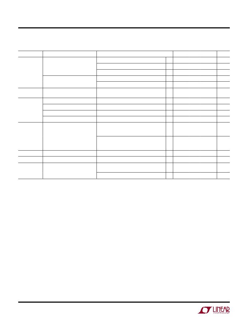
�ELECTRICAL� CHARACTERISTICS� The� l� denotes� the� specifications� which� apply� over� the� specified� operating�
�junction� temperature� range,� otherwise� specifications� are� at� T� A� =� 25°C� (Note� 2),� SV� IN� =� PV� INx� =� 3.3V,� R� T� =� 178k,� R� SRLIM� =� 40.2k,� unless�
�otherwise� specified.�
�SYMBOL�
�j� SW1–SW2�
�PARAMETER�
�Output� Phase� Shift� Between� SW1�
�and� SW2� (LTC3615)�
�CONDITIONS�
�V� PHASE� <� 0.15� ?� SV� IN�
�0.35� ?� SV� IN� <� V� PHASE� <� 0.65� ?� SV� IN�
�MIN�
�TYP�
�0�
�90�
�MAX�
�UNITS�
�Deg�
�Deg�
�V� PHASE� >� 0.85� ?� SV� IN�
�180�
�Deg�
�Output� Phase� Shift� Between� SW1�
�and� SW2� (LTC3615-1)�
�V� PHASE� <� 0.65� ?� SV� IN�
�V� PHASE� >� 0.85� ?� SV� IN�
�140�
�180�
�Deg�
�Deg�
�V� SRLIM�
�Voltage� at� SRLIM� to� Enable� DDR�
�Mode�
�(Note� 9)�
�SV� IN� –� 0.3�
�V�
�V� MODE�
�(Note� 9)�
�Internal� Burst� Mode� Operation�
�Pulse-Skipping� Mode�
�Forced� Continuous� Mode�
�External� Burst� Mode� Operation�
�SV� IN� – 0.3�
�1.1�
�0.5�
�0.3�
�SV� IN� ? 0.58�
�0.85�
�V�
�V�
�V�
�V�
�PGOOD�
�Power� Good� Voltage� Windows�
�TRACK/SSx� =� SV� IN� ,� Entering� Window�
�V� FBx� Ramping� Up�
�V� FBx� Ramping� Down�
�TRACK/SSx� =� SV� IN� ,� Leaving� Window�
�V� FBx� Ramping� Up�
�V� FBx� Ramping� Down�
�–3.5�
�3.5�
�–6�
�6�
�9�
�–9�
�11�
�–11�
�%�
�%�
�%�
�%�
�t� PGOOD�
�Power� Good� Blanking� Time�
�Entering/Leaving� Window�
�70�
�105�
�140�
�μs�
�R� PGOOD�
�Power� Good� Pull-Down� On-Resistance� I� =� 10mA�
�8�
�12�
�30�
�Ω�
�V� RUN�
�Enable� Pin�
�Input� High�
�Input� Low�
�l�
�l�
�1�
�0.4�
�V�
�V�
�Pull-Down� Resistance�
�4�
�M�
�Note� 1:� Stresses� beyond� those� listed� under� Absolute� Maximum� Ratings�
�may� cause� permanent� damage� to� the� device.� Exposure� to� any� Absolute�
�Maximum� Rating� condition� for� extended� periods� may� affect� device�
�reliability� and� lifetime.�
�Note� 2:� The� LTC3615/LTC3615-1� are� tested� under� pulsed� load� conditions�
�such� that� T� J� ≈� T� A� .� The� LTC3615E/LTC3615E-1� are� guaranteed� to� meet�
�performance� specifications� over� the� 0°C� to� 85°C� operating� junction�
�temperature� range.� Specifications� over� the� –40°C� to� 125°C� operating�
�junction� temperature� range� are� assured� by� design,� characterization� and�
�correlation� with� statistical� process� controls.� The� LTC3615I/LTC3615I-1�
�are� guaranteed� to� meet� specifications� over� the� –40°C� to� 125°C� operating�
�junction� temperature� range.� The� LTC3615H/LTC3615H-1� are� guaranteed�
�to� meet� specifications� over� the� –40°C� to� 150°C� operating� temperature�
�range.� The� LTC3615MP/LTC3615MP-1� are� tested� and� guaranteed� to� meet�
�specifications� over� the� full� –55°C� to� 150°C� operating� junction� temperature�
�range.� High� junction� temperatures� degrade� operating� lifetime;� operating�
�lifetime� is� derated� for� junction� temperatures� greater� than� 125°C.� Note� that�
�the� maximum� ambient� temperature� consistent� with� these� specifications�
�is� determined� by� specific� operating� conditions� in� conjunction� with� board�
�layout,� the� rated� package� thermal� impedance� and� other� environmental�
�factors.� The� junction� temperature� (T� J� ,� in� °C)� is� calculated� from� the� ambient�
�temperature�
�(T� A� ,� in� °C)� and� power� dissipation� (P� D� ,� in� watts)� according� to� the� formula:�
�T� J� =� T� A� +� (P� D� ?� θ� JA� )�
�where� θ� JA� (in� °C/W)� is� the� package� thermal� impedance.�
�Note� 3:� This� parameter� is� tested� in� a� feedback� loop� which� servos� V� FB1,2� to�
�the� midpoint� for� the� error� amplifier� (V� ITH1,2� =� 0.75V).�
�Note� 4:� External� compensation� on� ITH� pin.�
�Note� 5:� Tying� the� ITH� pin� to� SV� IN� enables� internal� compensation� and� AVP�
�mode� for� the� selected� channel.�
�Note� 6:� Dynamic� supply� current� is� higher� due� to� the� internal� gate� charge�
�being� delivered� at� the� switching� frequency.�
�Note� 7:� See� description� of� the� TRACK/SS� pin� in� the� Pin� Functions� section.�
�Note� 8:� When� sourcing� current,� the� average� output� current� is� defined�
�as� flowing� out� of� the� SW� pin.� When� sinking� current,� the� average� output�
�current� is� defined� as� flowing� into� the� SW� pin.� Sinking� mode� requires� the�
�use� of� forced� continuous� mode.�
�Note� 9:� See� description� of� the� MODE� pin� in� the� Pin� Functions� section.�
�Note� 10:� Guaranteed� by� design� and� correlation� to� wafer� level�
�measurements� for� QFN� packages.�
�Note� 11:� This� IC� includes� overtemperature� protection� that� is� intended�
�to� protect� the� device� during� momentary� overload� conditions.� Junction�
�temperature� will� exceed� 150°C� when� overtemperature� protection� is� active.�
�Continuous� operation� above� the� specified� maximum� operating� junction�
�temperature� may� impair� device� reliability� or� permanently� damage� the�
�device.�
�4�
�For� more� information� www.linear.com/LTC3615�
�3615fb�
�相关PDF资料 |
PDF描述 |
|---|---|
| MAX6716AUTWGD2+T | IC SUPERVISOR MPU SOT23-6 |
| EGM15DTAS | CONN EDGECARD 30POS R/A .156 SLD |
| UPS2D010MED1TD | CAP ALUM 1UF 200V 20% RADIAL |
| MAX6715AUTYFD2+T | IC SUPERVISOR MPU SOT23-6 |
| MAX6716AUTTED2+T | IC SUPERVISOR MPU SOT23-6 |
相关代理商/技术参数 |
参数描述 |
|---|---|
| LTC3615IUFPBF | 制造商:Linear Technology 功能描述:Dual 4MHz 3A Synch Step-Down DC/DC QFN24 |
| LTC3615MPFE#PBF | 制造商:Linear Technology 功能描述:IC REG BUCK SYNC ADJ 3A 24TSSOP |
| LTC3615MPFE#TRPBF | 制造商:Linear Technology 功能描述:IC REG BUCK SYNC ADJ 3A 24TSSOP |
| LTC3615MPFE-1#PBF | 制造商:Linear Technology 功能描述:IC REG BUCK SYNC ADJ 3A 24TSSOP |
| LTC3615MPFE-1#TRPBF | 制造商:Linear Technology 功能描述:IC REG BUCK SYNC ADJ 3A 24TSSOP |
发布紧急采购,3分钟左右您将得到回复。