- 您现在的位置:买卖IC网 > PDF目录44992 > LTC3728IG (LINEAR TECHNOLOGY CORP) 3 A DUAL SWITCHING CONTROLLER, 590 kHz SWITCHING FREQ-MAX, PDSO28 PDF资料下载
参数资料
| 型号: | LTC3728IG |
| 厂商: | LINEAR TECHNOLOGY CORP |
| 元件分类: | 稳压器 |
| 英文描述: | 3 A DUAL SWITCHING CONTROLLER, 590 kHz SWITCHING FREQ-MAX, PDSO28 |
| 封装: | 0.209 INCH, PLASTIC, SSOP-28 |
| 文件页数: | 18/36页 |
| 文件大小: | 1661K |
| 代理商: | LTC3728IG |
第1页第2页第3页第4页第5页第6页第7页第8页第9页第10页第11页第12页第13页第14页第15页第16页第17页当前第18页第19页第20页第21页第22页第23页第24页第25页第26页第27页第28页第29页第30页第31页第32页第33页第34页第35页第36页
LTC3728
25
3728fg
APPLICATIONS INFORMATION
Voltage Positioning
Voltage positioning can be used to minimize peak-to-peak
output voltage excursions under worst-case transient
loading conditions. The open-loop DC gain of the control
loop is reduced depending upon the maximum load step
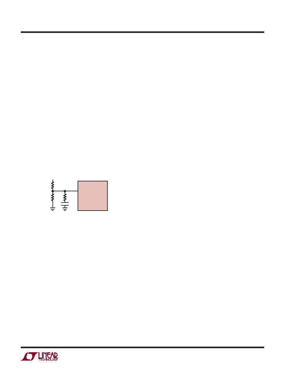
specications. Voltage positioning can easily be added to
the LTC3728 by loading the ITH pin with a resistive divider
having a Thevenin equivalent voltage source equal to the
midpoint operating voltage range of the error amplier, or
1.2V (see Figure 8).
The resistive load reduces the DC loop gain while main-
taining the linear control range of the error amplier. The
maximum output voltage deviation can theoretically be
reduced to half, or alternatively, the amount of output
capacitance can be reduced for a particular application.
A complete explanation is included in Design Solutions
10 (see www.linear.com).
Efciency Considerations
The percent efciency of a switching regulator is equal to
the output power divided by the input power times 100%.
It is often useful to analyze individual losses to determine
what is limiting the efciency and which change would
produce the most improvement. Percent efciency can
be expressed as:
%Efciency = 100% – (L1 + L2 + L3 + ...)
where L1, L2, etc. are the individual losses as a percent-
age of input power.
ITH
RC
RT1
INTVCC
CC
3728 F08
LTC3728
RT2
Figure 8. Active Voltage Positioning
Applied to the LTC3728
Although all dissipative elements in the circuit produce
losses, four main sources usually account for most
of the losses in LTC3728 circuits: 1) LTC3728 VIN cur-
rent (including loading on the 3.3V internal regulator),
2) INTVCC regulator current, 3) I2R losses, 4) Topside
MOSFET transition losses.
1. The VIN current has two components: the rst is the
DC supply current given in the Electrical Characteristics
table, which excludes MOSFET driver and control cur-
rents; the second is the current drawn from the 3.3V
linear regulator output. VIN current typically results in
a small (<0.1%) loss.
2. INTVCC current is the sum of the MOSFET driver and
control currents. The MOSFET driver current results
from switching the gate capacitance of the power
MOSFETs. Each time a MOSFET gate is switched from
low to high to low again, a packet of charge dQ
moves from INTVCC to ground. The resulting dQ/dt is
a current out of INTVCC that is typically much larger
than the control circuit current. In continuous mode,
IGATECHG = f(QT QB), where QT and QB are the gate
charges of the topside and bottom side MOSFETs.
Supplying INTVCC power through the EXTVCC switch
input from an output-derived source will scale the VIN
current required for the driver and control circuits by
a factor of (Duty Cycle)/(Efciency). For example, in a
20V to 5V application, 10mA of INTVCC current results
in approximately 2.5mA of VIN current. This reduces
the mid-current loss from 10% or more (if the driver
was powered directly from VIN) to only a few percent.
3. I2R losses are predicted from the DC resistances of the
fuse (if used), MOSFET, inductor, current sense resis-
tor, and input and output capacitor ESR. In continuous
mode, the average output current ows through L and
RSENSE, but is “chopped” between the topside MOSFET
and the synchronous MOSFET. If the two MOSFETs
have approximately the same RDS(ON), then the resis-
tance of one MOSFET can simply be summed with the
resistances of L, RSENSE and ESR to obtain I2R losses.
For example, if each RDS(ON) = 30mΩ, RL = 50mΩ,
相关PDF资料 |
PDF描述 |
|---|---|
| LTC3728LIUH-1#TR | 3 A DUAL SWITCHING CONTROLLER, 590 kHz SWITCHING FREQ-MAX, PQCC32 |
| LTC3728LIGN-1 | 3 A DUAL SWITCHING CONTROLLER, 590 kHz SWITCHING FREQ-MAX, PDSO28 |
| LTC3731HUH#TRPBF | 5 A SWITCHING CONTROLLER, 750 kHz SWITCHING FREQ-MAX, PQCC32 |
| LTC3731HUH#PBF | 5 A SWITCHING CONTROLLER, 750 kHz SWITCHING FREQ-MAX, PQCC32 |
| LTC3772BETS8#PBF | 1 A SWITCHING CONTROLLER, 650 kHz SWITCHING FREQ-MAX, PDSO8 |
相关代理商/技术参数 |
参数描述 |
|---|---|
| LTC3728IG#PBF | 功能描述:IC REG CTRLR BUCK PWM CM 28-SSOP RoHS:是 类别:集成电路 (IC) >> PMIC - 稳压器 - DC DC 切换控制器 系列:PolyPhase® 标准包装:4,500 系列:PowerWise® PWM 型:控制器 输出数:1 频率 - 最大:1MHz 占空比:95% 电源电压:2.8 V ~ 5.5 V 降压:是 升压:无 回扫:无 反相:无 倍增器:无 除法器:无 Cuk:无 隔离:无 工作温度:-40°C ~ 125°C 封装/外壳:6-WDFN 裸露焊盘 包装:带卷 (TR) 配用:LM1771EVAL-ND - BOARD EVALUATION LM1771 其它名称:LM1771SSDX |
| LTC3728IG#TRPBF | 功能描述:IC REG CTRLR BUCK PWM CM 28-SSOP RoHS:是 类别:集成电路 (IC) >> PMIC - 稳压器 - DC DC 切换控制器 系列:PolyPhase® 标准包装:4,500 系列:PowerWise® PWM 型:控制器 输出数:1 频率 - 最大:1MHz 占空比:95% 电源电压:2.8 V ~ 5.5 V 降压:是 升压:无 回扫:无 反相:无 倍增器:无 除法器:无 Cuk:无 隔离:无 工作温度:-40°C ~ 125°C 封装/外壳:6-WDFN 裸露焊盘 包装:带卷 (TR) 配用:LM1771EVAL-ND - BOARD EVALUATION LM1771 其它名称:LM1771SSDX |
| LTC3728IUH#PBF | 功能描述:IC REG CTRLR BUCK PWM CM 32-QFN RoHS:是 类别:集成电路 (IC) >> PMIC - 稳压器 - DC DC 切换控制器 系列:PolyPhase® 标准包装:4,500 系列:PowerWise® PWM 型:控制器 输出数:1 频率 - 最大:1MHz 占空比:95% 电源电压:2.8 V ~ 5.5 V 降压:是 升压:无 回扫:无 反相:无 倍增器:无 除法器:无 Cuk:无 隔离:无 工作温度:-40°C ~ 125°C 封装/外壳:6-WDFN 裸露焊盘 包装:带卷 (TR) 配用:LM1771EVAL-ND - BOARD EVALUATION LM1771 其它名称:LM1771SSDX |
| LTC3728IUH#TRPBF | 功能描述:IC REG CTRLR BUCK PWM CM 32-QFN RoHS:是 类别:集成电路 (IC) >> PMIC - 稳压器 - DC DC 切换控制器 系列:PolyPhase® 标准包装:4,500 系列:PowerWise® PWM 型:控制器 输出数:1 频率 - 最大:1MHz 占空比:95% 电源电压:2.8 V ~ 5.5 V 降压:是 升压:无 回扫:无 反相:无 倍增器:无 除法器:无 Cuk:无 隔离:无 工作温度:-40°C ~ 125°C 封装/外壳:6-WDFN 裸露焊盘 包装:带卷 (TR) 配用:LM1771EVAL-ND - BOARD EVALUATION LM1771 其它名称:LM1771SSDX |
| LTC3728LCGN | 功能描述:IC REG CTRLR BUCK PWM CM 28-SSOP RoHS:否 类别:集成电路 (IC) >> PMIC - 稳压器 - DC DC 切换控制器 系列:PolyPhase® 标准包装:4,500 系列:PowerWise® PWM 型:控制器 输出数:1 频率 - 最大:1MHz 占空比:95% 电源电压:2.8 V ~ 5.5 V 降压:是 升压:无 回扫:无 反相:无 倍增器:无 除法器:无 Cuk:无 隔离:无 工作温度:-40°C ~ 125°C 封装/外壳:6-WDFN 裸露焊盘 包装:带卷 (TR) 配用:LM1771EVAL-ND - BOARD EVALUATION LM1771 其它名称:LM1771SSDX |
发布紧急采购,3分钟左右您将得到回复。