- 您现在的位置:买卖IC网 > PDF目录1832 > LTC3787EUFD#PBF (Linear Technology)IC REG CTRLR BST PWM CM 28-QFN PDF资料下载
参数资料
| 型号: | LTC3787EUFD#PBF |
| 厂商: | Linear Technology |
| 文件页数: | 4/36页 |
| 文件大小: | 0K |
| 描述: | IC REG CTRLR BST PWM CM 28-QFN |
| 标准包装: | 73 |
| 系列: | PolyPhase® |
| PWM 型: | 电流模式 |
| 输出数: | 1 |
| 频率 - 最大: | 850kHz |
| 占空比: | 100% |
| 电源电压: | 4.5 V ~ 38 V |
| 降压: | 无 |
| 升压: | 是 |
| 回扫: | 无 |
| 反相: | 无 |
| 倍增器: | 无 |
| 除法器: | 无 |
| Cuk: | 无 |
| 隔离: | 无 |
| 工作温度: | -40°C ~ 125°C |
| 封装/外壳: | 28-WFQFN 裸露焊盘 |
| 包装: | 管件 |
第1页第2页第3页当前第4页第5页第6页第7页第8页第9页第10页第11页第12页第13页第14页第15页第16页第17页第18页第19页第20页第21页第22页第23页第24页第25页第26页第27页第28页第29页第30页第31页第32页第33页第34页第35页第36页
�� �
�
�LTC3787�
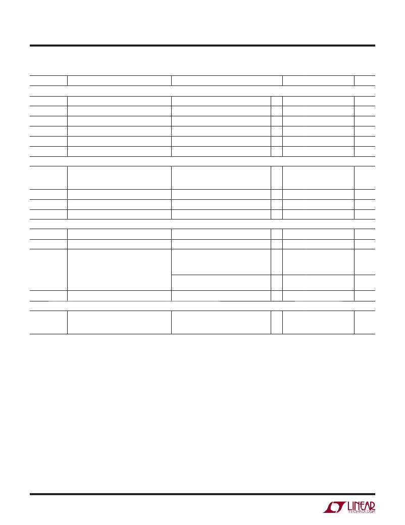
�ELECTRICAL� CHARACTERISTICS� The� l� denotes� the� specifications� which� apply� over� the� specified� operating�
�junction� temperature� range,� otherwise� specifications� are� at� T� A� =� 25°C,� VBIAS� =� 12V,� unless� otherwise� noted� (Note� 2).�
�SYMBOL�
�PARAMETER�
�CONDITIONS�
�MIN�
�TYP�
�MAX�
�UNITS�
�INTV� CC� Linear� Regulator�
�V� INTVCC(VIN)�
�VLDO� INT�
�V� INTVCC(EXT)�
�VLDO� EXT�
�Internal� V� CC� Voltage�
�INTV� CC� Load� Regulation�
�Internal� V� CC� Voltage�
�INTV� CC� Load� Regulation�
�6V� <� V� BIAS� <� 38V,� V� EXTVCC� =� 0�
�I� CC� =� 0mA� to� 50mA�
�V� EXTVCC� =� 6V�
�I� CC� =� 0mA� to� 40mA,� V� EXTVCC� =� 6V�
�5.2�
�5.2�
�5.4�
�0.5�
�5.4�
�0.5�
�5.6�
�2�
�5.6�
�2�
�V�
�%�
�V�
�%�
�V� EXTVCC�
�EXTV� CC� Switchover� Voltage�
�EXTV� CC� Ramping� Positive�
�l�
�4.5�
�4.8�
�5�
�V�
�V� LDOHYS�
�EXTV� CC� Hysteresis�
�250�
�mV�
�Oscillator� and� Phase-Locked� Loop�
�f� PROG�
�Programmable� Frequency�
�R� FREQ� =� 25k�
�105�
�kHz�
�R� FREQ� =� 60k�
�R� FREQ� =� 100k�
�335�
�400�
�760�
�465�
�kHz�
�kHz�
�f� LOW�
�f� HIGH�
�Lowest� Fixed� Frequency�
�Highest� Fixed� Frequency�
�V� FREQ� =� 0V�
�V� FREQ� =� INTV� CC�
�320�
�488�
�350�
�535�
�380�
�585�
�kHz�
�kHz�
�f� SYNC�
�Synchronizable� Frequency�
�PLLIN/MODE� =� External� Clock�
�l�
�75�
�850�
�kHz�
�PGOOD� Output�
�V� PGL�
�I� PGOOD�
�PGOOD� Voltage� Low�
�PGOOD� Leakage� Current�
�I� PGOOD� =� 2mA�
�V� PGOOD� =� 5V�
�0.2�
�0.4�
�±1�
�V�
�μA�
�V� PGOOD�
�PGOOD� Trip� Level�
�V� FB� with� Respect� to� Set� Regulated� Voltage�
�V� FB� Ramping� Negative�
�Hysteresis�
�V� FB� Ramping� Positive�
�Hysteresis�
�–12�
�8�
�–10�
�2.5�
�10�
�2.5�
�–8�
�12�
�%�
�%�
�%�
�%�
�t� PGOOD(DELAY)�
�PGOOD� Delay�
�PGOOD� Going� High� to� Low�
�25�
�μs�
�BOOST1� and� BOOST2� Charge� Pump�
�I� BOOST1,2�
�BOOST� Charge� Pump� Available� Output�
�V� SW1,2� =� 12V;� V� BOOST1,2� –� V� SW1,2� =� 4.5V;�
�55�
�μA�
�Current�
�FREQ� =� 0V,� Forced� Continuous� or�
�Pulse-Skipping� Mode�
�Note� 1:� Stresses� beyond� those� listed� under� Absolute� Maximum� Ratings�
�may� cause� permanent� damage� to� the� device.� Exposure� to� any� Absolute�
�Maximum� Rating� condition� for� extended� periods� may� affect� device�
�reliability� and� lifetime.�
�Note� 2:� The� LTC3787� is� tested� under� pulsed� load� conditions� such� that�
�T� J� ≈� T� A� .� The� LTC3787E� is� guaranteed� to� meet� specifications� from�
�0°C� to� 85°C� junction� temperature.� Specifications� over� the� –40°C� to�
�125°C� operating� junction� temperature� range� are� assured� by� design,�
�characterization� and� correlation� with� statistical� process� controls.� The�
�LTC3787I� is� guaranteed� over� the� –40°C� to� 125°C� operating� junction�
�temperature� range,� the� LTC3787H� is� guaranteed� over� the� –40°C� to� 150°C�
�operating� temperature� range� and� the� LTC3787MP� is� tested� and� guaranteed�
�over� the� full� –55°C� to� 150°C� operating� junction� temperature� range.� High�
�junction� temperatures� degrade� operating� lifetimes;� operating� lifetime�
�is� derated� for� junction� temperatures� greater� than� 125°C.� Note� that� the�
�maximum� ambient� temperature� consistent� with� these� specifications� is�
�determined� by� specific� operating� conditions� in� conjunction� with� board�
�layout,� the� rated� package� thermal� impedance� and� other� environmental�
�factors.� The� junction� temperature� (T� J� ,� in� °C)� is� calculated� from� the� ambient�
�temperature� (T� A� ,� in� °C)� and� power� dissipation� (P� D� ,� in� Watts)� according� to�
�the� formula:� T� J� =� T� A� +� (P� D� ?� θ� JA� ),� where� θ� JA� =� 43°C/W� for� the� QFN� package�
�and� θ� JA� =� 90°C/W� for� the� SSOP� package.�
�Note� 3:� This� IC� includes� overtemperature� protection� that� is� intended� to�
�protect� the� device� during� momentary� overload� conditions.� The� maximum�
�rated� junction� temperature� will� be� exceeded� when� this� protection� is� active.�
�Continuous� operation� above� the� specified� absolute� maximum� operating�
�junction� temperature� may� impair� device� reliability� or� permanently� damage�
�the� device.�
�Note� 4:� The� LTC3787� is� tested� in� a� feedback� loop� that� servos� V� FB� to� the�
�output� of� the� error� amplifier� while� maintaining� I� TH� at� the� midpoint� of� the�
�current� limit� range.�
�Note� 5:� Dynamic� supply� current� is� higher� due� to� the� gate� charge� being�
�delivered� at� the� switching� frequency.�
�Note� 6:� Rise� and� fall� times� are� measured� using� 10%� and� 90%� levels.� Delay�
�times� are� measured� using� 50%� levels.�
�Note� 7:� see� Minimum� On-Time� Considerations� in� the� Applications�
�Information� section.�
�3787fc�
�4�
�相关PDF资料 |
PDF描述 |
|---|---|
| LTC3788IUH#TRPBF | IC REG CTRLR BST PWM CM 32-QFN |
| LTC3789EGN#PBF | IC REG CTRLR BST PWM CM 28-SSOP |
| LTC3801BES6#TRM | IC REG CTRLR BUCK PWM TSOT23-6 |
| LTC3802EGN | IC REG CTRLR BUCK PWM VM 28-SSOP |
| LTC3803MPS6-3#TRMPBF | IC REG CTRLR FLYBK PWM TSOT23-6 |
相关代理商/技术参数 |
参数描述 |
|---|---|
| LTC3787HGN#PBF | 功能描述:IC REG CTRLR BST PWM CM 28-SSOP RoHS:是 类别:集成电路 (IC) >> PMIC - 稳压器 - DC DC 切换控制器 系列:PolyPhase® 标准包装:4,500 系列:PowerWise® PWM 型:控制器 输出数:1 频率 - 最大:1MHz 占空比:95% 电源电压:2.8 V ~ 5.5 V 降压:是 升压:无 回扫:无 反相:无 倍增器:无 除法器:无 Cuk:无 隔离:无 工作温度:-40°C ~ 125°C 封装/外壳:6-WDFN 裸露焊盘 包装:带卷 (TR) 配用:LM1771EVAL-ND - BOARD EVALUATION LM1771 其它名称:LM1771SSDX |
| LTC3787HGN#TRPBF | 功能描述:IC REG CTRLR BST PWM CM 28-SSOP RoHS:是 类别:集成电路 (IC) >> PMIC - 稳压器 - DC DC 切换控制器 系列:PolyPhase® 标准包装:4,500 系列:PowerWise® PWM 型:控制器 输出数:1 频率 - 最大:1MHz 占空比:95% 电源电压:2.8 V ~ 5.5 V 降压:是 升压:无 回扫:无 反相:无 倍增器:无 除法器:无 Cuk:无 隔离:无 工作温度:-40°C ~ 125°C 封装/外壳:6-WDFN 裸露焊盘 包装:带卷 (TR) 配用:LM1771EVAL-ND - BOARD EVALUATION LM1771 其它名称:LM1771SSDX |
| LTC3787HUFD#PBF | 功能描述:IC REG CTRLR BST PWM CM 28-QFN RoHS:是 类别:集成电路 (IC) >> PMIC - 稳压器 - DC DC 切换控制器 系列:PolyPhase® 标准包装:4,500 系列:PowerWise® PWM 型:控制器 输出数:1 频率 - 最大:1MHz 占空比:95% 电源电压:2.8 V ~ 5.5 V 降压:是 升压:无 回扫:无 反相:无 倍增器:无 除法器:无 Cuk:无 隔离:无 工作温度:-40°C ~ 125°C 封装/外壳:6-WDFN 裸露焊盘 包装:带卷 (TR) 配用:LM1771EVAL-ND - BOARD EVALUATION LM1771 其它名称:LM1771SSDX |
| LTC3787HUFD#TRPBF | 功能描述:IC REG CTRLR BST PWM CM 28-QFN RoHS:是 类别:集成电路 (IC) >> PMIC - 稳压器 - DC DC 切换控制器 系列:PolyPhase® 标准包装:4,500 系列:PowerWise® PWM 型:控制器 输出数:1 频率 - 最大:1MHz 占空比:95% 电源电压:2.8 V ~ 5.5 V 降压:是 升压:无 回扫:无 反相:无 倍增器:无 除法器:无 Cuk:无 隔离:无 工作温度:-40°C ~ 125°C 封装/外壳:6-WDFN 裸露焊盘 包装:带卷 (TR) 配用:LM1771EVAL-ND - BOARD EVALUATION LM1771 其它名称:LM1771SSDX |
| LTC3787IGN#PBF | 功能描述:IC REG CTRLR BST PWM CM 28-SSOP RoHS:是 类别:集成电路 (IC) >> PMIC - 稳压器 - DC DC 切换控制器 系列:PolyPhase® 标准包装:4,500 系列:PowerWise® PWM 型:控制器 输出数:1 频率 - 最大:1MHz 占空比:95% 电源电压:2.8 V ~ 5.5 V 降压:是 升压:无 回扫:无 反相:无 倍增器:无 除法器:无 Cuk:无 隔离:无 工作温度:-40°C ~ 125°C 封装/外壳:6-WDFN 裸露焊盘 包装:带卷 (TR) 配用:LM1771EVAL-ND - BOARD EVALUATION LM1771 其它名称:LM1771SSDX |
发布紧急采购,3分钟左右您将得到回复。