- 您现在的位置:买卖IC网 > PDF目录15274 > LTC3802EGN#PBF (Linear Technology)IC REG CTRLR BUCK PWM VM 28-SSOP PDF资料下载
参数资料
| 型号: | LTC3802EGN#PBF |
| 厂商: | Linear Technology |
| 文件页数: | 21/28页 |
| 文件大小: | 0K |
| 描述: | IC REG CTRLR BUCK PWM VM 28-SSOP |
| 标准包装: | 49 |
| 系列: | PolyPhase® |
| PWM 型: | 电压模式 |
| 输出数: | 2 |
| 频率 - 最大: | 850kHz |
| 占空比: | 92% |
| 电源电压: | 3 V ~ 30 V |
| 降压: | 是 |
| 升压: | 无 |
| 回扫: | 无 |
| 反相: | 无 |
| 倍增器: | 无 |
| 除法器: | 无 |
| Cuk: | 无 |
| 隔离: | 无 |
| 工作温度: | -40°C ~ 85°C |
| 封装/外壳: | 28-SSOP(0.154",3.90mm 宽) |
| 包装: | 管件 |
第1页第2页第3页第4页第5页第6页第7页第8页第9页第10页第11页第12页第13页第14页第15页第16页第17页第18页第19页第20页当前第21页第22页第23页第24页第25页第26页第27页第28页
�� �
�
�LTC3802�
�APPLICATIO� S� I� FOR� ATIO�
�floating,� it� sits� at� around� 2V� and� the� internal� phase-locked�
�loop� synchronizes� TG1’s� falling� edge� to� the� falling� edge� of�
�the� PLLIN� signal.� When� PHASEMD� is� high,� these� two�
�signals� are� 90� °� out� of� phase.� TG1� and� TG2� remains� 180� °�
�out� of� phase� independent� of� PHASEMD� input.�
�The� PHASEMD� signal� together� with� the� PLL� circuit� can� be�
�used� to� synchronize� an� additional� LTC3802� power� supply�
�circuit� to� provide� a� 4-phase,� 4-output� solution.� Compared�
�to� an� in-phase� multiple� controller� solution,� the� LTC3802’s�
�4-phase� design� reduces� the� input� capacitor� ripple� current�
�requirements� and� efficiency� losses� because� the� peak�
�current� drawn� from� the� input� capacitor� is� spaced� out�
�within� the� switching� cycle.�
�EXTERNAL� COMPONENTS� SELECTION�
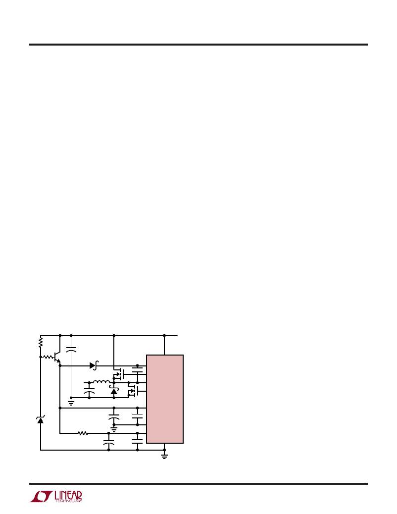
�V� CC� and� PV� CC� Power� Supplies�
�Power� for� the� top� and� bottom� MOSFET� drivers� is� derived�
�from� the� PV� CC� pin;� the� internal� controller� circuitry� is� de-�
�rived� from� the� V� CC� pin.� Under� typical� operating� conditions,�
�the� total� current� consumption� at� these� two� pins� should� be�
�well� below� 100mA.� Hence,� PV� CC� and� V� CC� can� be� connected�
�to� an� external� auxiliary� 5V� power� supply.� If� an� auxiliary�
�supply� is� not� available,� a� simple� zener� diode� and� a� darlington�
�NPN� buffer� can� be� used� to� power� up� these� two� pins� as�
�shown� in� Figure� 7.� To� prevent� switching� noise� from� cou-�
�pling� to� the� sensitive� analog� control� circuitry,� V� CC� should�
�have� a� 10� μ� F� bypassed� capacitor� close� to� the� device.� The�
�BiCMOS� process� that� allows� the� LTC3802� to� include� large�
�on-chip� MOSFET� drivers� also� limits� the� maximum� PV� CC�
�and� V� CC� voltage� to� 7V.� This� limits� the� practical� maximum�
�auxiliary� supply� to� a� loosely� regulated� 7V� rail.� If� V� CC� drops�
�below� 2.5V� or� PV� CC� drops� below� V� CC� by� more� than� 1V,� the�
�LTC3802� goes� into� undervoltage� lockout� and� prevents� the�
�power� switches� from� turning� on.�
�Top� MOSFET� Driver� Supply�
�An� external� bootstrap� capacitor,� C� CP� ,� connected� to� the�
�BOOST� pin� supplies� the� gate� drive� voltage� for� the� topside�
�MOSFET.� This� capacitor� is� charged� through� diode� DCP�
�from� PV� CC� when� the� switch� node� is� low.� When� the� top�
�MOSFET� turns� on,� the� switch� node� rises� to� V� IN� and� the�
�BOOST� pin� rises� to� approximately� V� IN� +� PV� CC� .� The� boost�
�capacitor� needs� to� store� about� 100� times� the� gate� charge�
�required� by� the� top� MOSFET.� In� most� applications� a� 0.1� μ� F�
�to� 1� μ� F,� X5R� or� X7R� dielectric� capacitor� is� adequate.�
�Power� MOSFET� Selection�
�The� LTC3802� requires� two� external� N-channel� power�
�MOSFETs,� one� for� the� top� (main)� switch� and� one� for� the�
�bottom� (synchronous)� switch.� Important� parameters� for�
�the� power� MOSFETs� are� the� threshold� voltage� V� (GS)TH� ,�
�breakdown� voltage� V� (BR)DSS� ,� maximum� current� I� DS(MAX)� ,�
�on-resistance� R� DS(ON)� and� input� capacitance.�
�R� Z�
�2k�
�100� ?�
�Q1�
�+�
�C� IN�
�V� OUT�
�+�
�DCP�
�L�
�QT�
�C� CP�
�V� INFF�
�BOOST�
�TG�
�SW�
�V� IN�
�The� gate� drive� voltage� is� set� by� the� 5V� PV� CC� supply.�
�Consequently,� logic-level� threshold� MOSFETs� must� be�
�used� in� LTC3802� applications.� If� the� PV� CC� voltage� is�
�expected� to� drop� below� 5V,� then� sub-logic� level� threshold�
�MOSFETs� should� be� considered.� Pay� close� attention� to� the�
�V� (BR)DSS� specification,� because� most� logic-level� MOSFETs�
�are� limited� to� 30V� or� less.� The� MOSFETs� selected� should�
�V� Z�
�5.6V�
�C� OUT�
�10� ?�
�D1�
�+�
�10� μ� F�
�+�
�10� μ� F�
�QB�
�0.1� μ� F�
�0.1� μ� F�
�BG�
�LTC3802�
�PV� CC�
�PGND�
�V� CC�
�SGND�
�3802� F07�
�have� a� V� (BR)DSS� rating� greater� than� the� maximum� input�
�voltage� and� some� margin� should� be� added� for� transients�
�and� spikes.� The� MOSFETs� selected� should� also� have� an�
�I� DS(MAX)� rating� of� at� least� two� times� the� maximum� power�
�stage� output� current.� Still,� this� may� not� be� a� sufficient�
�margin� so� it� is� advisable� to� calculate� the� MOSFET’s� junc-�
�tion� temperature� to� ensure� that� it� is� not� exceeded.�
�Q1:� ZETEX� FZT603�
�V� Z� :� MM5Z6V2ST1�
�Figure� 7.� LTC3802� Power� Supply� Inputs�
�The� LTC3802� uses� the� bottom� MOSFET� as� the� current�
�sense� element,� particular� attention� must� be� paid� to� its�
�3802f�
�21�
�相关PDF资料 |
PDF描述 |
|---|---|
| LTC1149CS-5#PBF | IC REG CTRLR BUCK PWM CM 16-SOIC |
| LTC1149CS-5 | IC REG CTRLR BUCK PWM CM 16-SOIC |
| EYM22DRST | CONN EDGECARD 44POS DIP .156 SLD |
| EGM22DRST | CONN EDGECARD 44POS DIP .156 SLD |
| LTC3708EUH | IC REG CTRLR BUCK PWM CM 32-QFN |
相关代理商/技术参数 |
参数描述 |
|---|---|
| LTC3802EUH | 功能描述:IC REG CTRLR BUCK PWM VM 32-QFN RoHS:否 类别:集成电路 (IC) >> PMIC - 稳压器 - DC DC 切换控制器 系列:PolyPhase® 标准包装:4,500 系列:PowerWise® PWM 型:控制器 输出数:1 频率 - 最大:1MHz 占空比:95% 电源电压:2.8 V ~ 5.5 V 降压:是 升压:无 回扫:无 反相:无 倍增器:无 除法器:无 Cuk:无 隔离:无 工作温度:-40°C ~ 125°C 封装/外壳:6-WDFN 裸露焊盘 包装:带卷 (TR) 配用:LM1771EVAL-ND - BOARD EVALUATION LM1771 其它名称:LM1771SSDX |
| LTC3802EUH#PBF | 功能描述:IC REG CTRLR BUCK PWM VM 32-QFN RoHS:是 类别:集成电路 (IC) >> PMIC - 稳压器 - DC DC 切换控制器 系列:PolyPhase® 标准包装:4,500 系列:PowerWise® PWM 型:控制器 输出数:1 频率 - 最大:1MHz 占空比:95% 电源电压:2.8 V ~ 5.5 V 降压:是 升压:无 回扫:无 反相:无 倍增器:无 除法器:无 Cuk:无 隔离:无 工作温度:-40°C ~ 125°C 封装/外壳:6-WDFN 裸露焊盘 包装:带卷 (TR) 配用:LM1771EVAL-ND - BOARD EVALUATION LM1771 其它名称:LM1771SSDX |
| LTC3802EUH#TR | 功能描述:IC REG CTRLR BUCK PWM VM 32-QFN RoHS:否 类别:集成电路 (IC) >> PMIC - 稳压器 - DC DC 切换控制器 系列:PolyPhase® 标准包装:4,500 系列:PowerWise® PWM 型:控制器 输出数:1 频率 - 最大:1MHz 占空比:95% 电源电压:2.8 V ~ 5.5 V 降压:是 升压:无 回扫:无 反相:无 倍增器:无 除法器:无 Cuk:无 隔离:无 工作温度:-40°C ~ 125°C 封装/外壳:6-WDFN 裸露焊盘 包装:带卷 (TR) 配用:LM1771EVAL-ND - BOARD EVALUATION LM1771 其它名称:LM1771SSDX |
| LTC3802EUH#TRPBF | 功能描述:IC REG CTRLR BUCK PWM VM 32-QFN RoHS:是 类别:集成电路 (IC) >> PMIC - 稳压器 - DC DC 切换控制器 系列:PolyPhase® 标准包装:4,500 系列:PowerWise® PWM 型:控制器 输出数:1 频率 - 最大:1MHz 占空比:95% 电源电压:2.8 V ~ 5.5 V 降压:是 升压:无 回扫:无 反相:无 倍增器:无 除法器:无 Cuk:无 隔离:无 工作温度:-40°C ~ 125°C 封装/外壳:6-WDFN 裸露焊盘 包装:带卷 (TR) 配用:LM1771EVAL-ND - BOARD EVALUATION LM1771 其它名称:LM1771SSDX |
| LTC3803ES6 | 制造商:Linear Technology 功能描述:DC DC Cntrlr Single-OUT Flyback Controller 9.2V to 75V Input 6-Pin TSOT-23 |
发布紧急采购,3分钟左右您将得到回复。