- 您现在的位置:买卖IC网 > PDF目录15299 > LTC3809EMSE#PBF (Linear Technology)IC REG CTRLR BUCK PWM CM 10-MSOP PDF资料下载
参数资料
| 型号: | LTC3809EMSE#PBF |
| 厂商: | Linear Technology |
| 文件页数: | 19/24页 |
| 文件大小: | 0K |
| 描述: | IC REG CTRLR BUCK PWM CM 10-MSOP |
| 标准包装: | 50 |
| PWM 型: | 电流模式 |
| 输出数: | 1 |
| 频率 - 最大: | 825kHz |
| 占空比: | 100% |
| 电源电压: | 2.75 V ~ 9.8 V |
| 降压: | 是 |
| 升压: | 无 |
| 回扫: | 无 |
| 反相: | 无 |
| 倍增器: | 无 |
| 除法器: | 无 |
| Cuk: | 无 |
| 隔离: | 无 |
| 工作温度: | -40°C ~ 85°C |
| 封装/外壳: | 10-TFSOP,10-MSOP(0.118",3.00mm 宽)裸露焊盘 |
| 包装: | 管件 |
| 产品目录页面: | 1336 (CN2011-ZH PDF) |
�� �
�
�LTC3809�
�APPLICATIONS� INFORMATION�
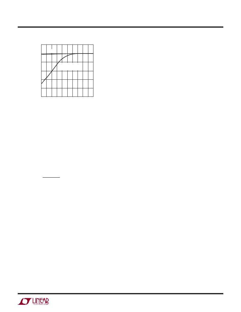
�105�
�limiting� ef� ?ciency� and� which� change� would� produce� the�
�100�
�95�
�90�
�85�
�80�
�75�
�V� REF�
�MAXIMUM�
�SENSE� VOLTAGE�
�2.0� 2.1� 2.2� 2.3� 2.4� 2.5� 2.6� 2.7� 2.8� 2.9� 3.0�
�INPUT� VOLTAGE� (V)�
�most� improvement.� Ef� ?ciency� can� be� expressed� as:�
�Ef� ?ciency� =� 100%� –� (L1� +� L2� +� L3� +� …)�
�where� L1,� L2,� etc.� are� the� individual� losses� as� a� percent-�
�age� of� input� power.�
�Although� all� dissipative� elements� in� the� circuit� produce�
�losses,� four� main� sources� usually� account� for� most� of� the�
�losses� in� LTC3809� circuits:� 1)� LTC3809� DC� bias� current,�
�2)� MOSFET� gate-charge� current,� 3)� I� 2� R� losses� and�
�4)� transition� losses.�
�3809� F09�
�Figure� 9.� Line� Regulation� of� V� REF� and� Maximum� Sense� Voltage�
�Minimum� On-Time� Considerations�
�Minimum� on-time,� t� ON(MIN)� is� the� smallest� amount� of� time�
�that� the� LTC3809� is� capable� of� turning� the� top� P-channel�
�MOSFET� on.� It� is� determined� by� internal� timing� delays� and�
�the� gate� charge� required� to� turn� on� the� top� MOSFET.� Low�
�duty� cycle� and� high� frequency� applications� may� approach�
�the� minimum� on-time� limit� and� care� should� be� taken� to�
�ensure� that:�
�1)� The� V� IN� (pin)� current� is� the� DC� supply� current,� given�
�in� the� Electrical� Characteristics,� which� excludes� MOSFET�
�driver� currents.� V� IN� current� results� in� a� small� loss� that�
�increases� with� V� IN� .�
�2)� MOSFET� gate-charge� current� results� from� switching�
�the� gate� capacitance� of� the� power� MOSFET.� Each� time� a�
�MOSFET� gate� is� switched� from� low� to� high� to� low� again,�
�a� packet� of� charge� dQ� moves� from� V� IN� to� ground.� The�
�resulting� dQ/dt� is� a� current� out� of� V� IN� ,� which� is� typically�
�much� larger� than� the� DC� supply� current.� In� continuous�
�mode,� I� GATECHG� =� f� ?� Q� P� .�
�t� ON� (� MIN� )� <�
�V� OUT�
�f� OSC� ?� V� IN�
�3)� I� 2� R� losses� are� calculated� from� the� DC� resistances� of� the�
�MOSFETs,� inductor� and/or� sense� resistor.� In� continuous�
�mode,� the� average� output� current� ?ows� through� L� but� is�
�If� the� duty� cycle� falls� below� what� can� be� accommodated�
�by� the� minimum� on-time,� the� LTC3809� will� begin� to� skip�
�cycles� (unless� forced� continuous� mode� is� selected).� The�
�output� voltage� will� continue� to� be� regulated,� but� the� ripple�
�current� and� ripple� voltage� will� increase.� The� minimum� on-�
�time� for� the� LTC3809� is� typically� about� 210ns.� However,�
�as� the� peak� sense� voltage� (I� L(PEAK� )� ?� R� DS(ON)� )� decreases,�
�the� minimum� on-time� gradually� increases� up� to� about�
�260ns.� This� is� of� particular� concern� in� forced� continu-�
�ous� applications� with� low� ripple� current� at� light� loads.� If�
�forced� continuous� mode� is� selected� and� the� duty� cycle�
�falls� below� the� minimum� on� time� requirement,� the� output�
�“chopped”� between� the� top� P-channel� MOSFET� and� the�
�bottom� N-channel� MOSFET.� The� MOSFET� R� DS(ON)� mul-�
�tiplied� by� duty� cycle� can� be� summed� with� the� resistance�
�of� L� to� obtain� I� 2� R� losses.�
�4)� Transition� losses� apply� to� the� external� MOSFET� and�
�increase� with� higher� operating� frequencies� and� input�
�voltages.� Transition� losses� can� be� estimated� from:�
�Transition� Loss� =� 2� ?� V� IN2� ?� I� O(MAX)� ?� C� RSS� ?� f�
�Other� losses,� including� C� IN� and� C� OUT� ESR� dissipative� losses�
�and� inductor� core� losses,� generally� account� for� less� than�
�2%� total� additional� loss.�
�will� be� regulated� by� overvoltage� protection.�
�Checking� Transient� Response�
�Ef� ?ciency� Considerations�
�The� ef� ?ciency� of� a� switching� regulator� is� equal� to� the� output�
�power� divided� by� the� input� power� times� 100%.� It� is� often�
�useful� to� analyze� individual� losses� to� determine� what� is�
�The� regulator� loop� response� can� be� checked� by� looking�
�at� the� load� transient� response.� Switching� regulators� take�
�several� cycles� to� respond� to� a� step� in� load� current.� When�
�a� load� step� occurs,� V� OUT� immediately� shifts� by� an� amount�
�3809fc�
�19�
�相关PDF资料 |
PDF描述 |
|---|---|
| ISC1210EBR27J | INDUCTOR WW 270NH 5% 1210 |
| RMM08DSAI | CONN EDGECARD 16POS R/A .156 SLD |
| LTC3810EUH-5#TRPBF | IC REG CTRLR BUCK PWM CM 32-QFN |
| VE-274-EW-F1 | CONVERTER MOD DC/DC 48V 100W |
| RSM12DRTI | CONN EDGECARD 24POS DIP .156 SLD |
相关代理商/技术参数 |
参数描述 |
|---|---|
| LTC3809IDD-1#PBF | 功能描述:IC REG CTRLR BUCK PWM CM 10-DFN RoHS:是 类别:集成电路 (IC) >> PMIC - 稳压器 - DC DC 切换控制器 系列:- 标准包装:2,500 系列:- PWM 型:电流模式 输出数:1 频率 - 最大:500kHz 占空比:96% 电源电压:4 V ~ 36 V 降压:无 升压:是 回扫:无 反相:无 倍增器:无 除法器:无 Cuk:无 隔离:无 工作温度:-40°C ~ 125°C 封装/外壳:24-WQFN 裸露焊盘 包装:带卷 (TR) |
| LTC3809IDD-1#TRPBF | 功能描述:IC REG CTRLR BUCK PWM CM 10-DFN RoHS:是 类别:集成电路 (IC) >> PMIC - 稳压器 - DC DC 切换控制器 系列:- 标准包装:2,500 系列:- PWM 型:电流模式 输出数:1 频率 - 最大:500kHz 占空比:96% 电源电压:4 V ~ 36 V 降压:无 升压:是 回扫:无 反相:无 倍增器:无 除法器:无 Cuk:无 隔离:无 工作温度:-40°C ~ 125°C 封装/外壳:24-WQFN 裸露焊盘 包装:带卷 (TR) |
| LTC3809IMSE-1#PBF | 功能描述:IC REG CTRLR BUCK PWM CM 10-MSOP RoHS:是 类别:集成电路 (IC) >> PMIC - 稳压器 - DC DC 切换控制器 系列:- 标准包装:2,500 系列:- PWM 型:电流模式 输出数:1 频率 - 最大:500kHz 占空比:96% 电源电压:4 V ~ 36 V 降压:无 升压:是 回扫:无 反相:无 倍增器:无 除法器:无 Cuk:无 隔离:无 工作温度:-40°C ~ 125°C 封装/外壳:24-WQFN 裸露焊盘 包装:带卷 (TR) |
| LTC3809IMSE-1#TRPBF | 功能描述:IC REG CTRLR BUCK PWM CM 10-MSOP RoHS:是 类别:集成电路 (IC) >> PMIC - 稳压器 - DC DC 切换控制器 系列:- 标准包装:2,500 系列:- PWM 型:电流模式 输出数:1 频率 - 最大:500kHz 占空比:96% 电源电压:4 V ~ 36 V 降压:无 升压:是 回扫:无 反相:无 倍增器:无 除法器:无 Cuk:无 隔离:无 工作温度:-40°C ~ 125°C 封装/外壳:24-WQFN 裸露焊盘 包装:带卷 (TR) |
| LTC3810EG#PBF | 功能描述:IC REG CTRLR BUCK PWM CM 28-SSOP RoHS:是 类别:集成电路 (IC) >> PMIC - 稳压器 - DC DC 切换控制器 系列:- 特色产品:LM3753/54 Scalable 2-Phase Synchronous Buck Controllers 标准包装:1 系列:PowerWise® PWM 型:电压模式 输出数:1 频率 - 最大:1MHz 占空比:81% 电源电压:4.5 V ~ 18 V 降压:是 升压:无 回扫:无 反相:无 倍增器:无 除法器:无 Cuk:无 隔离:无 工作温度:-5°C ~ 125°C 封装/外壳:32-WFQFN 裸露焊盘 包装:Digi-Reel® 产品目录页面:1303 (CN2011-ZH PDF) 其它名称:LM3754SQDKR |
发布紧急采购,3分钟左右您将得到回复。