- 您现在的位置:买卖IC网 > PDF目录44993 > LTC3810EG (LINEAR TECHNOLOGY CORP) SWITCHING CONTROLLER, PDSO28 PDF资料下载
参数资料
| 型号: | LTC3810EG |
| 厂商: | LINEAR TECHNOLOGY CORP |
| 元件分类: | 稳压器 |
| 英文描述: | SWITCHING CONTROLLER, PDSO28 |
| 封装: | 5.30 MM, PLASTIC, SSOP-28 |
| 文件页数: | 8/36页 |
| 文件大小: | 495K |
| 代理商: | LTC3810EG |
第1页第2页第3页第4页第5页第6页第7页当前第8页第9页第10页第11页第12页第13页第14页第15页第16页第17页第18页第19页第20页第21页第22页第23页第24页第25页第26页第27页第28页第29页第30页第31页第32页第33页第34页第35页第36页
LTC3810
16
3810fb
The most important parameter in high voltage applications
is breakdown voltage BVDSS. Both the top and bottom
MOSFETs will see full input voltage plus any additional
ringing on the switch node across its drain-to-source dur-
ing its off-time and must be chosen with the appropriate
breakdown specication. Since most MOSFETs in the 60V
to 100V range have higher thresholds (typically VGS(MIN)
≥ 6V), the LTC3810 is designed to be used with a 6.2V to
14V gate drive supply (DRVCC pin).
For maximum efciency, on-resistance RDS(ON) and input
capacitance should be minimized. Low RDS(ON) minimizes
conduction losses and low input capacitance minimizes
transition losses. MOSFET input capacitance is a combi-
nation of several components but can be taken from the
typical “gate charge” curve included on most data sheets
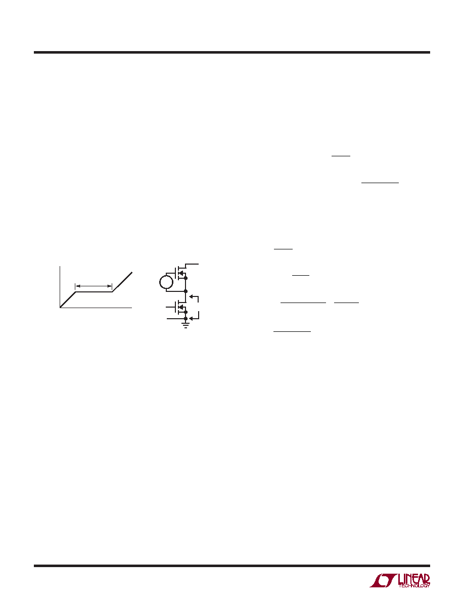
(Figure 6).
The curve is generated by forcing a constant input cur-
rent into the gate of a common source, current source
loaded stage and then plotting the gate voltage versus
time. The initial slope is the effect of the gate-to-source
and the gate-to-drain capacitance. The at portion of the
curve is the result of the Miller multiplication effect of the
drain-to-gate capacitance as the drain drops the voltage
across the current source load. The upper sloping line is
due to the drain-to-gate accumulation capacitance and
the gate-to-source capacitance. The Miller charge (the
increase in coulombs on the horizontal axis from a to b
while the curve is at) is specied for a given VDS drain
voltage, but can be adjusted for different VDS voltages by
multiplying by the ratio of the application VDS to the curve
specied VDS values. A way to estimate the CMILLER term
is to take the change in gate charge from points a and b
on a manufacturers data sheet and divide by the stated
VDS voltage specied. CMILLER is the most important se-
lection criteria for determining the transition loss term in
the top MOSFET but is not directly specied on MOSFET
data sheets. CRSS and COS are specied sometimes but
denitions of these parameters are not included.
When the controller is operating in continuous mode the
duty cycles for the top and bottom MOSFETs are given by:
MainSwitchDutyCycle
=
VOUT
VIN
SynchronousSwitchDutyCycle
=
VIN –VOUT
VIN
The power dissipation for the main and synchronous
MOSFETs at maximum output current are given by:
PTOP =
VOUT
VIN
IMAX
()2(
T )RDS(ON) +
VIN
2 IMAX
2
(RDR)(CMILLER)
1
VCC –VTH(IL)
+
1
VTH(IL)
(f)
PBOT =
VIN –VOUT
VIN
(IMAX)
2(
T )RDS(0N)
where
ρT is the temperature dependency of RDS(ON), RDR
is the effective top driver resistance (approximately 2
Ω at
VGS = VMILLER), VIN is the drain potential and the change
in drain potential in the particular application. VTH(IL) is
the data sheet specied typical gate threshold voltage
specied in the power MOSFET data sheet at the specied
drain current. CMILLER is the calculated capacitance using
the gate charge curve from the MOSFET data sheet and
the technique described above.
Both MOSFETs have I2R losses while the topside N-channel
equation incudes an additional term for transition losses,
which peak at the highest input voltage. For high input
voltage low duty cycle applications that are typical for the
LTC3810, transition losses are the dominate loss term and
therefore using higher RDS(ON) device with lower CMILLER
usually provides the highest efciency. The synchronous
MOSFET losses are greatest at high input voltage when
the top switch duty factor is low or during a short circuit
when the synchronous switch is on close to 100% of
Figure 6. Gate Charge Characteristic
APPLICATIONS INFORMATION
+
–
VDS
VIN
VGS
MILLER EFFECT
QIN
ab
CMILLER = (QB – QA)/VDS
VGS
V
+
–
3810 F06
相关PDF资料 |
PDF描述 |
|---|---|
| LTC3812EFE-5 | 1 A SWITCHING CONTROLLER, PDSO16 |
| LTC3812IFE-5#TR | 1 A SWITCHING CONTROLLER, PDSO16 |
| LTC3812EFE-5#TR | 1 A SWITCHING CONTROLLER, PDSO16 |
| LTC3812IFE-5 | 1 A SWITCHING CONTROLLER, PDSO16 |
| LTC3831IGN | SWITCHING CONTROLLER, 500 kHz SWITCHING FREQ-MAX, PDSO16 |
相关代理商/技术参数 |
参数描述 |
|---|---|
| LTC3810EG#PBF | 功能描述:IC REG CTRLR BUCK PWM CM 28-SSOP RoHS:是 类别:集成电路 (IC) >> PMIC - 稳压器 - DC DC 切换控制器 系列:- 特色产品:LM3753/54 Scalable 2-Phase Synchronous Buck Controllers 标准包装:1 系列:PowerWise® PWM 型:电压模式 输出数:1 频率 - 最大:1MHz 占空比:81% 电源电压:4.5 V ~ 18 V 降压:是 升压:无 回扫:无 反相:无 倍增器:无 除法器:无 Cuk:无 隔离:无 工作温度:-5°C ~ 125°C 封装/外壳:32-WFQFN 裸露焊盘 包装:Digi-Reel® 产品目录页面:1303 (CN2011-ZH PDF) 其它名称:LM3754SQDKR |
| LTC3810EG#TRPBF | 功能描述:IC REG CTRLR BUCK PWM CM 28-SSOP RoHS:是 类别:集成电路 (IC) >> PMIC - 稳压器 - DC DC 切换控制器 系列:- 标准包装:2,500 系列:- PWM 型:电流模式 输出数:1 频率 - 最大:500kHz 占空比:96% 电源电压:4 V ~ 36 V 降压:无 升压:是 回扫:无 反相:无 倍增器:无 除法器:无 Cuk:无 隔离:无 工作温度:-40°C ~ 125°C 封装/外壳:24-WQFN 裸露焊盘 包装:带卷 (TR) |
| LTC3810EUH-5#PBF | 功能描述:IC REG CTRLR BUCK PWM CM 32-QFN RoHS:是 类别:集成电路 (IC) >> PMIC - 稳压器 - DC DC 切换控制器 系列:- 标准包装:4,500 系列:PowerWise® PWM 型:控制器 输出数:1 频率 - 最大:1MHz 占空比:95% 电源电压:2.8 V ~ 5.5 V 降压:是 升压:无 回扫:无 反相:无 倍增器:无 除法器:无 Cuk:无 隔离:无 工作温度:-40°C ~ 125°C 封装/外壳:6-WDFN 裸露焊盘 包装:带卷 (TR) 配用:LM1771EVAL-ND - BOARD EVALUATION LM1771 其它名称:LM1771SSDX |
| LTC3810EUH-5#TRPBF | 功能描述:IC REG CTRLR BUCK PWM CM 32-QFN RoHS:是 类别:集成电路 (IC) >> PMIC - 稳压器 - DC DC 切换控制器 系列:- 标准包装:2,500 系列:- PWM 型:电流模式 输出数:1 频率 - 最大:500kHz 占空比:96% 电源电压:4 V ~ 36 V 降压:无 升压:是 回扫:无 反相:无 倍增器:无 除法器:无 Cuk:无 隔离:无 工作温度:-40°C ~ 125°C 封装/外壳:24-WQFN 裸露焊盘 包装:带卷 (TR) |
| LTC3810HUH-5#PBF | 功能描述:IC REG CTRLR BUCK PWM CM 32-QFN RoHS:是 类别:集成电路 (IC) >> PMIC - 稳压器 - DC DC 切换控制器 系列:- 标准包装:4,500 系列:PowerWise® PWM 型:控制器 输出数:1 频率 - 最大:1MHz 占空比:95% 电源电压:2.8 V ~ 5.5 V 降压:是 升压:无 回扫:无 反相:无 倍增器:无 除法器:无 Cuk:无 隔离:无 工作温度:-40°C ~ 125°C 封装/外壳:6-WDFN 裸露焊盘 包装:带卷 (TR) 配用:LM1771EVAL-ND - BOARD EVALUATION LM1771 其它名称:LM1771SSDX |
发布紧急采购,3分钟左右您将得到回复。