- 您现在的位置:买卖IC网 > PDF目录15293 > LTC3814IFE-5#TRPBF (Linear Technology)IC REG CTRLR BST PWM CM 16-TSSOP PDF资料下载
参数资料
| 型号: | LTC3814IFE-5#TRPBF |
| 厂商: | Linear Technology |
| 文件页数: | 12/30页 |
| 文件大小: | 0K |
| 描述: | IC REG CTRLR BST PWM CM 16-TSSOP |
| 标准包装: | 2,500 |
| PWM 型: | 电流模式 |
| 输出数: | 1 |
| 频率 - 最大: | 1MHz |
| 占空比: | 90% |
| 电源电压: | 4.5 V ~ 55 V |
| 降压: | 无 |
| 升压: | 是 |
| 回扫: | 无 |
| 反相: | 无 |
| 倍增器: | 无 |
| 除法器: | 无 |
| Cuk: | 无 |
| 隔离: | 无 |
| 工作温度: | -40°C ~ 125°C |
| 封装/外壳: | 16-TSSOP(0.173",4.40mm)裸露焊盘 |
| 包装: | 带卷 (TR) |
第1页第2页第3页第4页第5页第6页第7页第8页第9页第10页第11页当前第12页第13页第14页第15页第16页第17页第18页第19页第20页第21页第22页第23页第24页第25页第26页第27页第28页第29页第30页
�� �
�
�LTC3814-5�
�APPLICATIONS� INFORMATION�
�Power� MOSFET� Selection�
�The� LTC3814-5� requires� two� external� N-channel� power�
�MOSFETs,� one� for� the� bottom� (main)� switch� and� one� for�
�the� top� (synchronous)� switch.� Important� parameters� for�
�the� power� MOSFETs� are� the� breakdown� voltage� BV� DSS� ,�
�threshold� voltage� V� (GS)TH� ,� on-resistance� R� DS(ON)� ,� Miller�
�capacitance� and� maximum� current� I� DS(MAX)� .�
�Since� the� bottom� MOSFET� is� used� as� the� current� sense�
�element,� particular� attention� must� be� paid� to� its� on-resis-�
�tance.� MOSFET� on-resistance� is� typically� speci?ed� with�
�a� maximum� value� R� DS(ON)(MAX)� at� 25°C.� In� this� case,�
�additional� margin� is� required� to� accommodate� the� rise� in�
�MOSFET� on-resistance� with� temperature:�
�ing� its� off-time� and� must� be� chosen� with� the� appropriate�
�breakdown� speci?cation.� The� LTC3814-5� is� designed� to�
�be� used� with� a� 4.5V� to� 14V� gate� drive� supply� (INTV� CC� pin)�
�for� driving� logic-level� MOSFETs� (V� GS(MIN)� ≥� 4.5V).�
�For� maximum� ef?ciency,� on-resistance� R� DS(ON)� and� input�
�capacitance� should� be� minimized.� Low� R� DS(ON)� minimizes�
�conduction� losses� and� low� input� capacitance� minimizes�
�transition� losses.� MOSFET� input� capacitance� is� a� combi-�
�nation� of� several� components� but� can� be� taken� from� the�
�typical� “gate� charge”� curve� included� on� most� data� sheets�
�(Figure� 3).�
�V� OUT�
�R� DS(ON)(MAX)� =� SENSE�
�R�
�ρ� T�
�The� ρ� T� term� is� a� normalization� factor� (unity� at� 25°C)�
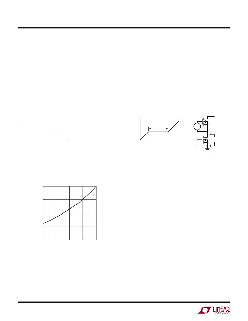
�V� GS�
�MILLER� EFFECT�
�a� b�
�Q� IN�
�C� MILLER� =� (Q� B� –� Q� A� )/V� DS�
�V�
�+�
�V� GS�
�–�
�+� V�
�–�
�DS�
�accounting� for� the� signi?cant� variation� in� on-resistance�
�with� temperature� (see� Figure� 2)� and� typically� varies�
�from� 0.4%/°C� to� 1.0%/°C� depending� on� the� particular�
�MOSFET� used.�
�2.0�
�1.5�
�1.0�
�0.5�
�38145� F03�
�Figure� 3.� Gate� Charge� Characteristic�
�The� curve� is� generated� by� forcing� a� constant� input� cur-�
�rent� into� the� gate� of� a� common� source,� current� source�
�loaded� stage� and� then� plotting� the� gate� voltage� versus�
�time.� The� initial� slope� is� the� effect� of� the� gate-to-source�
�and� the� gate-to-drain� capacitance.� The� ?at� portion� of� the�
�curve� is� the� result� of� the� Miller� multiplication� effect� of� the�
�drain-to-gate� capacitance� as� the� drain� drops� the� voltage�
�across� the� current� source� load.� The� upper� sloping� line� is�
�due� to� the� drain-to-gate� accumulation� capacitance� and�
�the� gate-to-source� capacitance.� The� Miller� charge� (the�
�increase� in� coulombs� on� the� horizontal� axis� from� a� to� b�
�while� the� curve� is� ?at)� is� speci?ed� for� a� given� V� DS� drain�
�0�
�–50�
�0� 50� 100�
�JUNCTION� TEMPERATURE� (°C)�
�150�
�38145� F02�
�voltage,� but� can� be� adjusted� for� different� V� DS� voltages� by�
�multiplying� by� the� ratio� of� the� application� V� DS� to� the� curve�
�speci?ed� V� DS� values.� A� way� to� estimate� the� C� MILLER� term�
�Figure� 2.� R� DS(ON)� vs� Temperature�
�The� most� important� parameter� in� high� voltage� applications�
�is� breakdown� voltage� BV� DSS� .� Both� the� top� and� bottom�
�MOSFETs� will� see� full� output� voltage� plus� any� additional�
�ringing� on� the� switch� node� across� its� drain-to-source� dur-�
�is� to� take� the� change� in� gate� charge� from� points� a� and� b�
�on� a� manufacturers� data� sheet� and� divide� by� the� stated�
�V� DS� voltage� speci?ed.� C� MILLER� is� the� most� important� se-�
�lection� criteria� for� determining� the� transition� loss� term� in�
�the� top� MOSFET� but� is� not� directly� speci?ed� on� MOSFET�
�data� sheets.� C� RSS� and� C� OS� are� speci?ed� sometimes� but�
�de?nitions� of� these� parameters� are� not� included.�
�38145fc�
�12�
�相关PDF资料 |
PDF描述 |
|---|---|
| H2AAT-10102-Y4-ND | JUMPER-H1502TR/A2015Y/H1502TR 2" |
| LTC1625CS | IC REG CTRLR BUCK PWM CM 16-SOIC |
| H2AAT-10102-W4-ND | JUMPER-H1502TR/A2015W/H1502TR 2" |
| LTC3810IG#TRPBF | IC REG CTRLR BUCK PWM CM 28-SSOP |
| H2AAT-10102-V4-ND | JUMPER-H1502TR/A2015V/H1502TR 2" |
相关代理商/技术参数 |
参数描述 |
|---|---|
| LTC3816EFE#PBF | 功能描述:IC DC-DC CTLR S-PHASE 38TSSOP RoHS:是 类别:集成电路 (IC) >> PMIC - 稳压器 - 专用型 系列:- 标准包装:2,000 系列:- 应用:控制器,DSP 输入电压:4.5 V ~ 25 V 输出数:2 输出电压:最低可调至 1.2V 工作温度:-40°C ~ 85°C 安装类型:表面贴装 封装/外壳:30-TFSOP(0.173",4.40mm 宽) 供应商设备封装:30-TSSOP 包装:带卷 (TR) |
| LTC3816EFE#TRPBF | 功能描述:IC CONTROLLER S-PHASE 38TSSOP RoHS:是 类别:集成电路 (IC) >> PMIC - 稳压器 - 专用型 系列:- 标准包装:43 系列:- 应用:控制器,Intel VR11 输入电压:5 V ~ 12 V 输出数:1 输出电压:0.5 V ~ 1.6 V 工作温度:-40°C ~ 85°C 安装类型:表面贴装 封装/外壳:48-VFQFN 裸露焊盘 供应商设备封装:48-QFN(7x7) 包装:管件 |
| LTC3816EUHF#PBF | 功能描述:IC DC-DC CTLR S-PHASE 32QFN RoHS:是 类别:集成电路 (IC) >> PMIC - 稳压器 - 专用型 系列:- 标准包装:2,000 系列:- 应用:控制器,DSP 输入电压:4.5 V ~ 25 V 输出数:2 输出电压:最低可调至 1.2V 工作温度:-40°C ~ 85°C 安装类型:表面贴装 封装/外壳:30-TFSOP(0.173",4.40mm 宽) 供应商设备封装:30-TSSOP 包装:带卷 (TR) |
| LTC3816EUHF#TRPBF | 功能描述:IC CONTROLLER S-PHASE 32QFN RoHS:是 类别:集成电路 (IC) >> PMIC - 稳压器 - 专用型 系列:- 标准包装:43 系列:- 应用:控制器,Intel VR11 输入电压:5 V ~ 12 V 输出数:1 输出电压:0.5 V ~ 1.6 V 工作温度:-40°C ~ 85°C 安装类型:表面贴装 封装/外壳:48-VFQFN 裸露焊盘 供应商设备封装:48-QFN(7x7) 包装:管件 |
| LTC3816IFE#PBF | 功能描述:IC CONTROLLER S-PHASE 38TSSOP RoHS:是 类别:集成电路 (IC) >> PMIC - 稳压器 - 专用型 系列:- 标准包装:43 系列:- 应用:控制器,Intel VR11 输入电压:5 V ~ 12 V 输出数:1 输出电压:0.5 V ~ 1.6 V 工作温度:-40°C ~ 85°C 安装类型:表面贴装 封装/外壳:48-VFQFN 裸露焊盘 供应商设备封装:48-QFN(7x7) 包装:管件 |
发布紧急采购,3分钟左右您将得到回复。