- 您现在的位置:买卖IC网 > PDF目录69007 > LTC3823EUH#TR (LINEAR TECHNOLOGY CORP) 4 A SWITCHING CONTROLLER, 200 kHz SWITCHING FREQ-MAX, PQCC32 PDF资料下载
参数资料
| 型号: | LTC3823EUH#TR |
| 厂商: | LINEAR TECHNOLOGY CORP |
| 元件分类: | 稳压器 |
| 英文描述: | 4 A SWITCHING CONTROLLER, 200 kHz SWITCHING FREQ-MAX, PQCC32 |
| 封装: | 5 X 5 MM, PLASTIC, MO-220WHHD, QFN-32 |
| 文件页数: | 7/24页 |
| 文件大小: | 345K |
| 代理商: | LTC3823EUH#TR |
LTC3823
3823fb
on, the switch node rises to VIN and the BOOST pin rises
to approximately VIN + INTVCC. The boost capacitor needs
to store about 100 times the gate charge required by the
top MOSFET. In most applications 0.1F to 0.47F, X5R
or X7R dielectric capacitor is adequate.
Discontinuous Mode Operation and FCB Pin
The FCB pin determines whether the bottom MOSFET
remains on when current reverses in the inductor. Tying
this pin above its 0.6V threshold enables discontinuous
operation where the bottom MOSFET turns off when in-
ductor current reverses. The load current at which current
reverses and discontinuous operation begins depends on
the amplitude of the inductor ripple current and will vary
with changes in VIN. Tying the FCB pin below the 0.6V
threshold forces continuous synchronous operation, al-
lowing current to reverse at light loads and maintaining
high frequency operation. To prevent forcing current back
into the main power supply, potentially boosting the input
supply to a dangerous voltage level, forced continuous
mode of operation is disabled when the TRACK/SS volt-
age is 20% below the reference voltage during soft-start
or tracking up. Forced continuous mode of operation is
also disabled when the TRACK/SS voltage is below 0.1V
duringtrackingdownoperation.Duringthesetwoperiods,
the PGOOD signal is forced low.
In addition to providing a logic input to force continu-
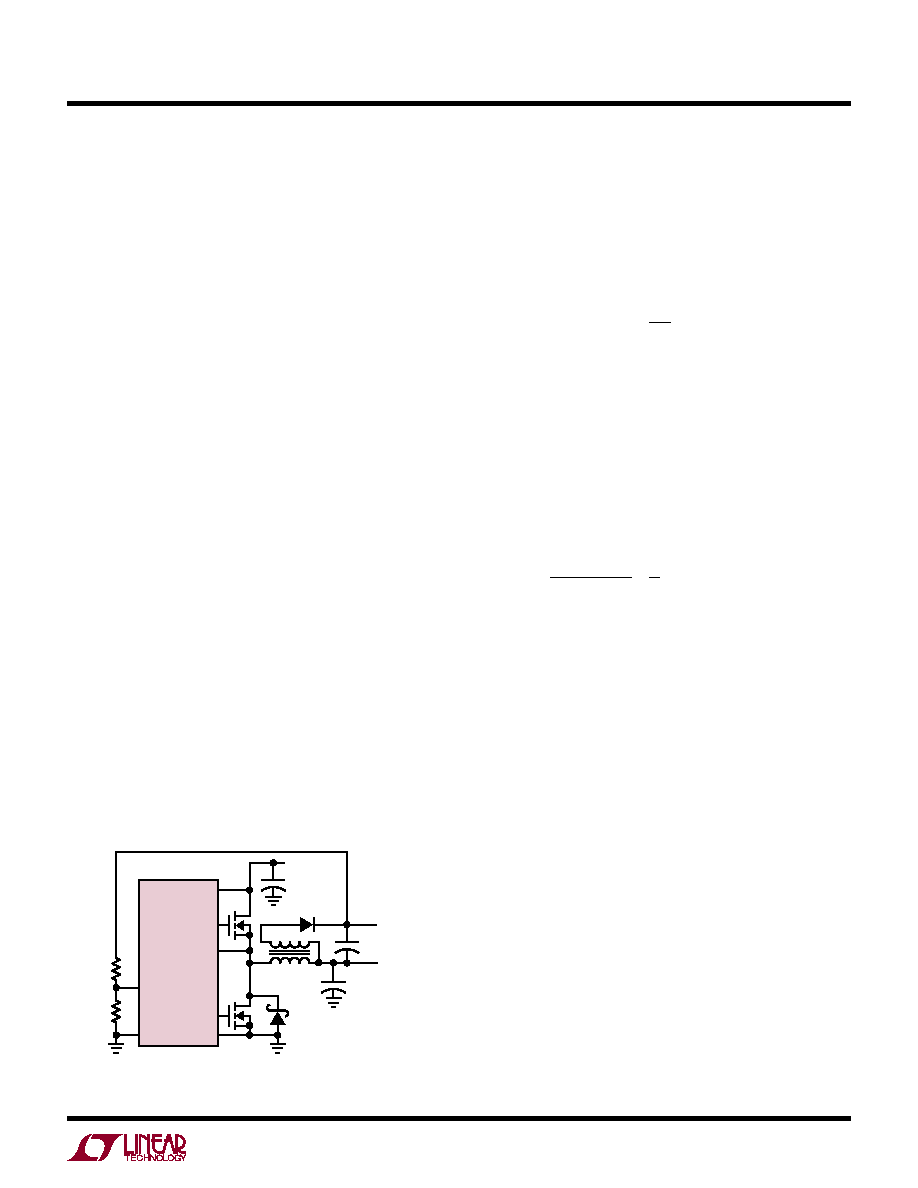
ous operation, the FCB pin provides a mean to maintain
a flyback winding output when the primary is operating
in discontinuous mode. The secondary output VOUT2 is
normally set as shown in Figure 5 by the turns ratio N
of the transformer. however, if the controller goes into
discontinuous mode and halts switching due to a light
primary load current, then VOUT2 will droop. An external
resistor divider from VOUT2 to the FCB pin sets a minimum
voltage VOUT2(MIN) below which continuous operation is
forced until VOUT2 has risen above its minimum.
V
R
OUT MIN
2
0 6 1
4
3
(
)
.
=
+
Fault Conditions: Current Limit and Foldback
The maximum inductor current is inherently limited in a
current mode controller by the maximum sense voltage.
In the LTC3823, the maximum sense voltage is controlled
by the voltage on the VRNG pin. With valley current control,
the maximum sense voltage and the sense resistance
determine the maximum allowed inductor valley current.
The corresponding output current limit is:
I
V
R
I
LIMIT
SNS MAX
DS ON
T
L
=
+ Δ
(
)
( ) ρ
1
2
The current limit value should be checked to ensure that
ILIMIT(MIN)>IOUT(MAX).Theminimumvalueofcurrentlimit
generally occurs with the largest VIN at the highest ambi-
ent temperature, conditions that cause the largest power
loss in the converter. Note that it is important to check for
self-consistency between the assumed MOSFET junction
temperature and the resulting value of ILIMIT which heats
the MOSFET switches.
Caution should be used when setting the current limit
based upon the RDS(ON) of the MOSFETs. The maximum
current limit is determined by the minimum MOSFET
on-resistance. Data sheets typically specify nominal
and maximum values for RDS(ON), but not a minimum.
A reasonable assumption is that the minimum RDS(ON)
lies the same percentage below the typical value as the
maximumliesaboveit.ConsulttheMOSFETmanufacturer
for further guidelines.
To further limit current in the event of a short circuit to
ground, the LTC3823 includes foldback current limiting.
If the output falls by more than 60%, then the maximum
sense voltage is progressively lowered to about one tenth
of its full value.
applications information
VIN
LTC3823
SGND
FCB
TG
SW
R3
R4
3823 F05
T1
1:N
BG
PGND
+
COUT2
1
F
VOUT1
VOUT2
VIN
+
CIN
1N4148
+
COUT
Figure 5. Secondary Output Loop
相关PDF资料 |
PDF描述 |
|---|---|
| LTC3823EGN#TR | 4 A SWITCHING CONTROLLER, 200 kHz SWITCHING FREQ-MAX, PDSO28 |
| LTC3827IUH | 3 A DUAL SWITCHING CONTROLLER, 580 kHz SWITCHING FREQ-MAX, PQCC32 |
| LTC3827IUH#TR | 3 A DUAL SWITCHING CONTROLLER, 580 kHz SWITCHING FREQ-MAX, PQCC32 |
| LTC4010EFE | 0.2 A BATTERY CHARGE CONTROLLER, 640 kHz SWITCHING FREQ-MAX, PDSO16 |
| LTC4065LXEDC#PBF | 1-CHANNEL POWER SUPPLY SUPPORT CKT, PDSO6 |
相关代理商/技术参数 |
参数描述 |
|---|---|
| LTC3823IGN#PBF | 功能描述:IC REG CTRLR BUCK PWM CM 28-SSOP RoHS:是 类别:集成电路 (IC) >> PMIC - 稳压器 - DC DC 切换控制器 系列:- 标准包装:2,000 系列:- PWM 型:电流模式 输出数:1 频率 - 最大:1MHz 占空比:50% 电源电压:9 V ~ 10 V 降压:无 升压:是 回扫:是 反相:无 倍增器:无 除法器:无 Cuk:无 隔离:无 工作温度:-40°C ~ 85°C 封装/外壳:8-TSSOP(0.173",4.40mm 宽) 包装:带卷 (TR) |
| LTC3823IGN#PBF | 制造商:Linear Technology 功能描述:IC SYNC STEP-DOWN DC/DC CTRL SSOP-28 |
| LTC3823IGN#TRPBF | 功能描述:IC REG CTRLR BUCK PWM CM 28-SSOP RoHS:是 类别:集成电路 (IC) >> PMIC - 稳压器 - DC DC 切换控制器 系列:- 标准包装:2,500 系列:- PWM 型:电流模式 输出数:1 频率 - 最大:500kHz 占空比:96% 电源电压:4 V ~ 36 V 降压:无 升压:是 回扫:无 反相:无 倍增器:无 除法器:无 Cuk:无 隔离:无 工作温度:-40°C ~ 125°C 封装/外壳:24-WQFN 裸露焊盘 包装:带卷 (TR) |
| LTC3823IUH#PBF | 功能描述:IC REG CTRLR BUCK PWM CM 32-QFN RoHS:是 类别:集成电路 (IC) >> PMIC - 稳压器 - DC DC 切换控制器 系列:- 特色产品:LM3753/54 Scalable 2-Phase Synchronous Buck Controllers 标准包装:1 系列:PowerWise® PWM 型:电压模式 输出数:1 频率 - 最大:1MHz 占空比:81% 电源电压:4.5 V ~ 18 V 降压:是 升压:无 回扫:无 反相:无 倍增器:无 除法器:无 Cuk:无 隔离:无 工作温度:-5°C ~ 125°C 封装/外壳:32-WFQFN 裸露焊盘 包装:Digi-Reel® 产品目录页面:1303 (CN2011-ZH PDF) 其它名称:LM3754SQDKR |
| LTC3823IUH#PBF | 制造商:Linear Technology 功能描述:IC SYNC STEP-DOWN DC/DC CONTROLLER QFN32 |
发布紧急采购,3分钟左右您将得到回复。