- 您现在的位置:买卖IC网 > PDF目录79926 > LTC3865IUH#PBF (LINEAR TECHNOLOGY CORP) DUAL SWITCHING CONTROLLER, 880 kHz SWITCHING FREQ-MAX, PQCC32 PDF资料下载
参数资料
| 型号: | LTC3865IUH#PBF |
| 厂商: | LINEAR TECHNOLOGY CORP |
| 元件分类: | 稳压器 |
| 英文描述: | DUAL SWITCHING CONTROLLER, 880 kHz SWITCHING FREQ-MAX, PQCC32 |
| 封装: | 5 X 5 MM, LEAD FREE, PLASTIC, MO-220WHHD, QFN-32 |
| 文件页数: | 15/38页 |
| 文件大小: | 400K |
| 代理商: | LTC3865IUH#PBF |
第1页第2页第3页第4页第5页第6页第7页第8页第9页第10页第11页第12页第13页第14页当前第15页第16页第17页第18页第19页第20页第21页第22页第23页第24页第25页第26页第27页第28页第29页第30页第31页第32页第33页第34页第35页第36页第37页第38页
LTC3865/LTC3865-1
22
3865fb
APPLICATIONS INFORMATION
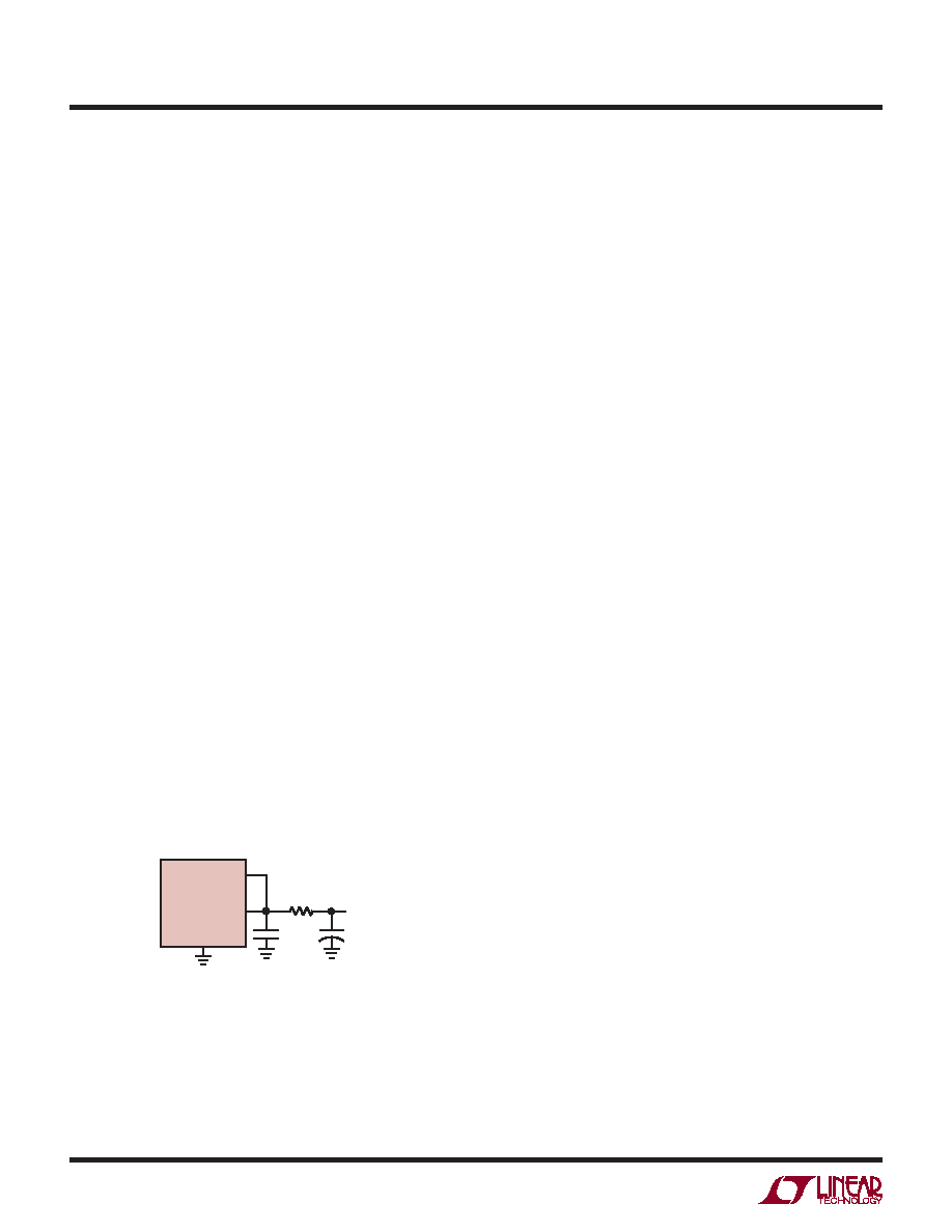
For applications where the main input power is below 5V,
tie the VIN and INTVCC pins together and tie the combined
pins to the 5V input with a 1Ω or 2.2Ω resistor as shown
in Figure 8 to minimize the voltage drop caused by the
gate charge current. This will override the INTVCC linear
regulator and will prevent INTVCC from dropping too low
due to the dropout voltage. Make sure the INTVCC voltage
is at or exceeds the RDS(ON) test voltage for the MOSFET
which is typically 4.5V for logic-level devices.
Topside MOSFET Driver Supply (CB, DB)
External bootstrap capacitors, CB, connected to the BOOST
pins supply the gate drive voltages for the topside MOSFETs.
Capacitor CB in the Functional Diagram is charged through
external diode DB from INTVCC when the SW pin is low.
When one of the topside MOSFETs is to be turned on, the
driver places the CB voltage across the gate source of the
desired MOSFET. This enhances the MOSFET and turns on
the topside switch. The switch node voltage, SW, rises to
VIN and the BOOST pin follows. With the topside MOSFET
on, the boost voltage is above the input supply: VBOOST
= VIN + VINTVCC. The value of the boost capacitor, CB,
needs to be 100 times that of the total input capacitance
of the topside MOSFET(s). The reverse breakdown of the
external Schottky diode must be greater than VIN(MAX).
When adjusting the gate drive level, the nal arbiter is the
total input current for the regulator. If a change is made
and the input current decreases, then the efciency has
improved. If there is no change in input current, then there
is no change in efciency.
Undervoltage Lockout
The LTC3865/LTC3865-1 have two functions that help
protect the controller in case of undervoltage conditions.
A precision UVLO comparator constantly monitors the
INTVCC voltage to ensure that an adequate gate-drive
voltage is present. It locks out the switching action when
INTVCC is below 3.3V. To prevent oscillation when there is
a disturbance on the INTVCC, the UVLO comparator has
550mV of precision hysteresis.
Another way to detect an undervoltage condition is to
monitor the VIN supply. Because the RUN pins have a
precision turn-on reference of 1.22V, one can use a resistor
divider to VIN to turn on the IC when VIN is high enough.
An extra 4.5μA of current ows out of the RUN pin once
the RUN pin voltage passes 1.22V. One can program the
hysteresis of the run comparator by adjusting the values
of the resistive divider. For accurate VIN undervoltage
detection, VIN needs to be higher than 4.5V.
CIN and COUT Selection
The selection of CIN is simplied by the 2-phase architec-
ture and its impact on the worst-case RMS current drawn
through the input network (battery/fuse/capacitor). It can be
shown that the worst-case capacitor RMS current occurs
when only one controller is operating. The controller with
the highest (VOUT)(IOUT) product needs to be used in the
formula below to determine the maximum RMS capacitor
current requirement. Increasing the output current drawn
from the other controller will actually decrease the input
RMS ripple current from its maximum value. The out-of-
phase technique typically reduces the input capacitor’s RMS
ripple current by a factor of 30% to 70% when compared
to a single phase power supply solution.
In continuous mode, the source current of the top MOSFET
is a square wave of duty cycle (VOUT)/(VIN). To prevent
large voltage transients, a low ESR capacitor sized for the
INTVCC
LTC3865
RVIN
1Ω
CIN
3865 F08
CINTVCC
4.7μF
5V
+
VIN
Figure 8. Setup for a 5V Input
相关PDF资料 |
PDF描述 |
|---|---|
| LM2575HVS-12EP | 3.2 A SWITCHING REGULATOR, 63 kHz SWITCHING FREQ-MAX, PSSO5 |
| LTC3872ETS8#PBF | SWITCHING CONTROLLER, 650 kHz SWITCHING FREQ-MAX, PDSO8 |
| LTC3850EGN | 0.1 A DUAL SWITCHING CONTROLLER, 860 kHz SWITCHING FREQ-MAX, PDSO28 |
| LT1933HS6#TR | 1.05 A SWITCHING REGULATOR, 600 kHz SWITCHING FREQ-MAX, PDSO6 |
| LC016AJ | 2-OUTPUT 16 W DC-DC REG PWR SUPPLY MODULE |
相关代理商/技术参数 |
参数描述 |
|---|---|
| LTC3866EFE#PBF | 功能描述:IC REG CTRLR BUCK PWM CM 24TSSOP RoHS:是 类别:集成电路 (IC) >> PMIC - 稳压器 - DC DC 切换控制器 系列:- 标准包装:2,000 系列:- PWM 型:电流模式 输出数:1 频率 - 最大:1MHz 占空比:50% 电源电压:9 V ~ 10 V 降压:无 升压:是 回扫:是 反相:无 倍增器:无 除法器:无 Cuk:无 隔离:无 工作温度:-40°C ~ 85°C 封装/外壳:8-TSSOP(0.173",4.40mm 宽) 包装:带卷 (TR) |
| LTC3866EFE#PBF | 制造商:Linear Technology 功能描述:BUCK REGULATOR CURRENT MODE SYNC TSSOP |
| LTC3866EFE#TRPBF | 功能描述:IC REG CTRLR BUCK PWM CM 24TSSOP RoHS:是 类别:集成电路 (IC) >> PMIC - 稳压器 - DC DC 切换控制器 系列:- 标准包装:2,500 系列:- PWM 型:电流模式 输出数:1 频率 - 最大:500kHz 占空比:96% 电源电压:4 V ~ 36 V 降压:无 升压:是 回扫:无 反相:无 倍增器:无 除法器:无 Cuk:无 隔离:无 工作温度:-40°C ~ 125°C 封装/外壳:24-WQFN 裸露焊盘 包装:带卷 (TR) |
| LTC3866EUF#PBF | 功能描述:IC REG CTRLR BUCK PWM CM 24-QFN RoHS:是 类别:集成电路 (IC) >> PMIC - 稳压器 - DC DC 切换控制器 系列:- 标准包装:2,500 系列:- PWM 型:电流模式 输出数:1 频率 - 最大:500kHz 占空比:96% 电源电压:4 V ~ 36 V 降压:无 升压:是 回扫:无 反相:无 倍增器:无 除法器:无 Cuk:无 隔离:无 工作温度:-40°C ~ 125°C 封装/外壳:24-WQFN 裸露焊盘 包装:带卷 (TR) |
| LTC3866EUF#TRPBF | 功能描述:IC REG CTRLR BUCK PWM CM 24-QFN RoHS:是 类别:集成电路 (IC) >> PMIC - 稳压器 - DC DC 切换控制器 系列:- 标准包装:2,500 系列:- PWM 型:电流模式 输出数:1 频率 - 最大:500kHz 占空比:96% 电源电压:4 V ~ 36 V 降压:无 升压:是 回扫:无 反相:无 倍增器:无 除法器:无 Cuk:无 隔离:无 工作温度:-40°C ~ 125°C 封装/外壳:24-WQFN 裸露焊盘 包装:带卷 (TR) |
发布紧急采购,3分钟左右您将得到回复。