- 您现在的位置:买卖IC网 > PDF目录32308 > LTC3873ITS8-5#TR (LINEAR TECHNOLOGY CORP) SWITCHING CONTROLLER, PDSO8 PDF资料下载
参数资料
| 型号: | LTC3873ITS8-5#TR |
| 厂商: | LINEAR TECHNOLOGY CORP |
| 元件分类: | 稳压器 |
| 英文描述: | SWITCHING CONTROLLER, PDSO8 |
| 封装: | 1 MM HEIGHT, PLASTIC, MO-193, TSOT-23, 8 PIN |
| 文件页数: | 10/16页 |
| 文件大小: | 170K |
| 代理商: | LTC3873ITS8-5#TR |
LTC3873-5
3
38735fb
Note 1: Stresses beyond those listed under Absolute Maximum Ratings
may cause permanent damage to the device. Exposure to any Absolute
Maximum Rating condition for extended periods may affect device
reliability and lifetime.
Note 2: The LTC3873E-5 is guaranteed to meet performance specications
from 0°C to 85°C. Specications over the –40°C to 85°C operating
temperature range are assured by design, characterization and correlation
with statistical process controls. The LTC3873I-5 is guaranteed to meet
performance specications over the full –40°C to 125°C operating
temperature range.
Note 3: TJ is calculated from the ambient temperature TA and power
dissipation PD according to the following formula:
TJ = TA + (PD θJA)
Note 4: The dynamic input supply current is higher due to power MOSFET
gate charging (QG fOSC). See Applications Information.
Note 5: The LTC3873-5 is tested in a feedback loop which servos VFB to
the reference voltage with the ITH pin forced to the midpoint of its voltage
range (0.7V ≤ VITH ≤ 1.9V, midpoint = 1.3V).
Note 6: Rise and fall times are measured at 10% and 90% levels.
VCC = 5.6V.
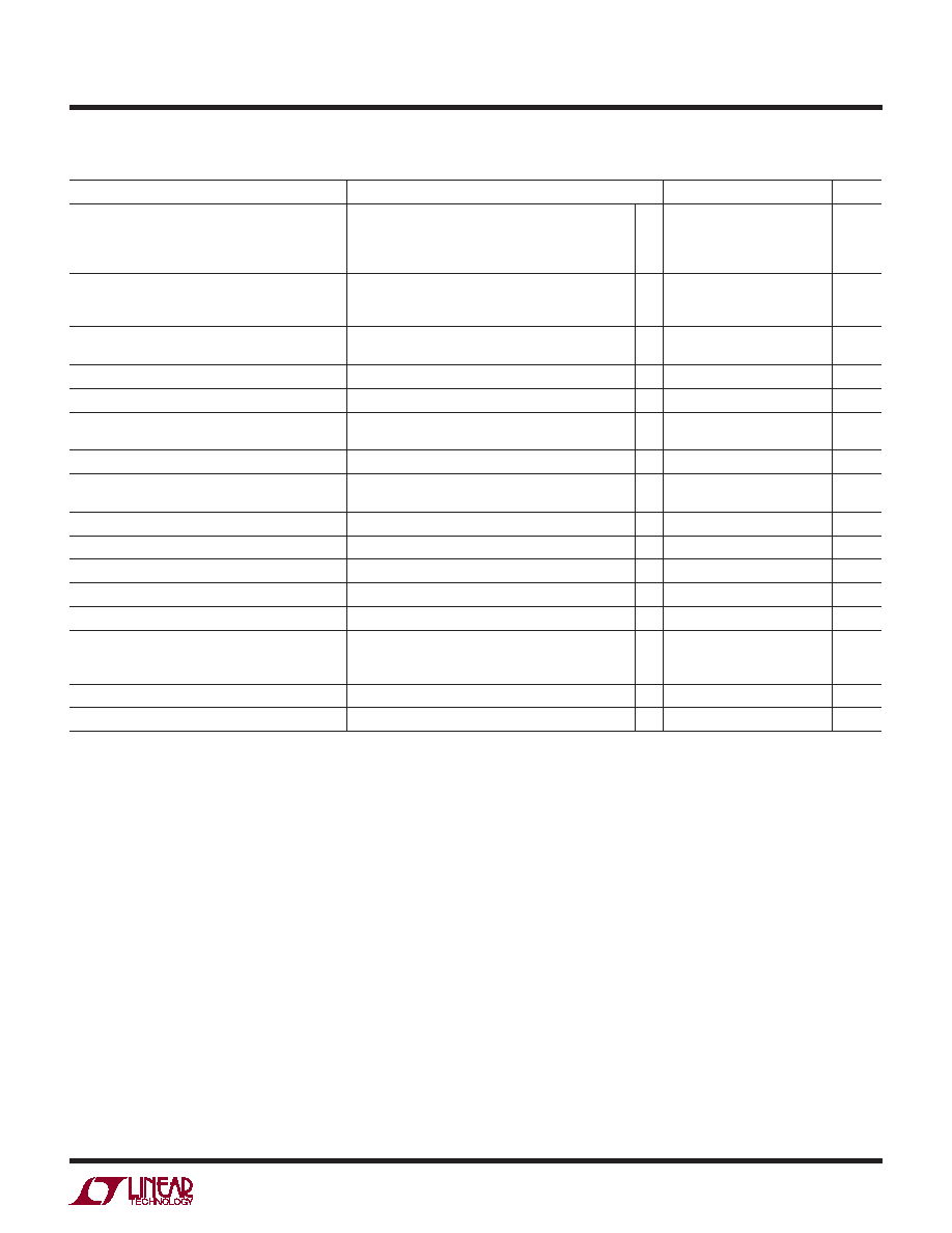
ELECTRICAL CHARACTERISTICS The l denotes the specications which apply over the full operating
temperature range, otherwise specications are at TA = 25°C. VCC = 5V unless otherwise noted. (Note 2)
PARAMETER
CONDITIONS
MIN
TYP
MAX
UNITS
Input DC Supply Current
Normal Operation
Shutdown
UVLO
Typicals at VCC = 5V (Note 4)
VITH = 1.9V
VRUN/SS = 0V
VCC = UVLO Threshold – 100mV, VRUN/SS = VCC
300
50
35
400
80
50
μA
Undervoltage Lockout Threshold
VCC Rising
VCC Falling
VCC Hysteresis
l
3.8
2.5
0.9
4.1
2.9
1.25
4.4
3.3
1.7
V
Shutdown Threshold (at RUN/SS)
VRUN/SS Falling
VRUN/SS Rising
l
0.5
0.6
0.7
0.8
0.9
1.0
V
Regulated Feedback Voltage
(Note 5)
l
1.182
1.2
1.218
V
Feedback Voltage Line Regulation
3.5V < VCC < 9V (Note 5)
0.1
mV/V
Feedback Voltage Load Regulation
VITH = 1.6V (Note 5)
VITH = 1V (Note 5)
0.05
–0.05
%
VFB Input Current
(Note 5)
25
50
nA
RUN/SS Pull Up Current
VRUN/SS = 0V
VRUN/SS = 1.3V
1.5
5
3
15
4.5
25
μA
Maximum Duty Cycle
70
78
84
%
ISLMAX, Peak Slope Compensation Current
20
μA
Oscillator Frequency
160
200
240
kHz
Gate Drive Rise Time
CLOAD = 3000pF (Note 6)
40
ns
Gate Drive Fall Time
CLOAD = 3000pF (Note 6)
40
ns
Peak Current Sense Voltage
IPRG = GND
IPRG = Float
IPRG = VIN
l
95
165
265
110
185
295
125
210
325
mV
VIN Shunt Regulator Voltage
IIN = 1mA, IIN = 25mA, VRUN/SS = 0V
l
9
9.3
9.6
V
Default Internal Soft-Start
3.3
ms
相关PDF资料 |
PDF描述 |
|---|---|
| LTC3873IDDB-5#PBF | SWITCHING CONTROLLER, PDSO8 |
| LTC3873ITS8-5 | SWITCHING CONTROLLER, PDSO8 |
| LTC3873ETS8-5 | SWITCHING CONTROLLER, 240 kHz SWITCHING FREQ-MAX, PDSO8 |
| LTM-9134-2 | INFRARED, REMOTE CONTROL SUPPORT CIRCUIT, SMA3 |
| LTM-9134-3 | INFRARED, REMOTE CONTROL SUPPORT CIRCUIT, SMA3 |
相关代理商/技术参数 |
参数描述 |
|---|---|
| LTC3874EUFD#PBF | 制造商:Linear Technology 功能描述:IC REG CTRLR BUCK PWM CM 28QFN |
| LTC3874EUFD#TRPBF | 制造商:Linear Technology 功能描述:IC REG CTRLR BUCK PWM CM 28QFN |
| LTC3874IUFD#PBF | 制造商:Linear Technology 功能描述:IC REG BUCK SYNC STEP-DOWN 28QFN |
| LTC3874IUFD#TRPBF | 制造商:Linear Technology 功能描述:IC REG CTRLR BUCK PWM CM 28QFN |
| LTC3876EFE#PBF | 功能描述:IC CTLR DC/DC DDR DUAL 38-TSSOP RoHS:是 类别:集成电路 (IC) >> PMIC - 稳压器 - 专用型 系列:- 标准包装:43 系列:- 应用:控制器,Intel VR11 输入电压:5 V ~ 12 V 输出数:1 输出电压:0.5 V ~ 1.6 V 工作温度:-40°C ~ 85°C 安装类型:表面贴装 封装/外壳:48-VFQFN 裸露焊盘 供应商设备封装:48-QFN(7x7) 包装:管件 |
发布紧急采购,3分钟左右您将得到回复。