- 您现在的位置:买卖IC网 > PDF目录80295 > LTC4012IUF-2#TRPBF (LINEAR TECHNOLOGY CORP) SWITCHING CONTROLLER, 633 kHz SWITCHING FREQ-MAX, PQCC20 PDF资料下载
参数资料
| 型号: | LTC4012IUF-2#TRPBF |
| 厂商: | LINEAR TECHNOLOGY CORP |
| 元件分类: | 稳压器 |
| 英文描述: | SWITCHING CONTROLLER, 633 kHz SWITCHING FREQ-MAX, PQCC20 |
| 封装: | 4 X 4 MM, 0.75 MM HEIGHT, LEAD FREE, PLASTIC, MO-220WGGD-1, QFN-20 |
| 文件页数: | 17/28页 |
| 文件大小: | 381K |
| 代理商: | LTC4012IUF-2#TRPBF |
第1页第2页第3页第4页第5页第6页第7页第8页第9页第10页第11页第12页第13页第14页第15页第16页当前第17页第18页第19页第20页第21页第22页第23页第24页第25页第26页第27页第28页
LTC4012/
LTC4012-1/LTC4012-2
4012fa
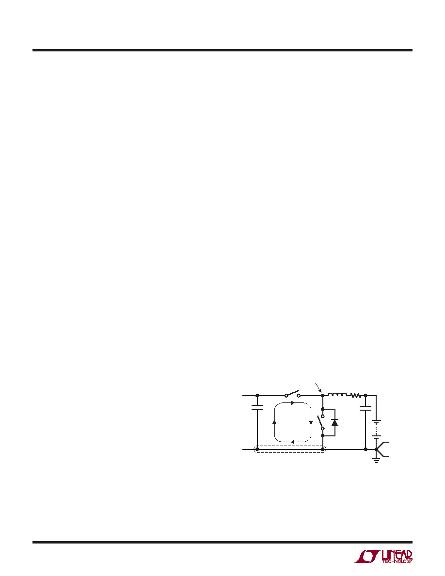
Figure 12. High Speed Switching Path
4012 F12
VBAT
L1
RSENSE
HIGH
FREQUENCY
CIRCULATING
PATH
BAT
ANALOG
GROUND
SYSTEM
GROUND
SWITCH NODE
CIN
SWITCHING GROUND
COUT
VIN
GND
D1
+
The LTC4012 can be soft-started with the compensation
capacitor on the ITH pin. At start-up, ITH will quickly rise
to about 0.25V, then ramp up at a rate set by the com-
pensation capacitor and the 40A ITH bias current. The
full programmed charge current will be reached when ITH
reaches approximately 2V. With a 0.1F capacitor, the time
to reach full charge current is usually greater than 1.5ms.
This capacitor can be increased if longer start-up times
are required, but loop bandwidth and dynamic response
will be reduced.
INTVDD Regulator Output
Bypass the INTVDD regulator output to GND with a low
ESR X5R or X7R ceramic capacitor with a value of 0.47F
or larger. The capacitor used to build the BOOST supply
(C2 in Figure 11) can serve as this bypass. Do not draw
more than 30mA from this regulator for the host system,
governed by IC power dissipation.
Calculating IC Power Dissipation
The user should ensure that the maximum rated junction
temperatureisnotexceededunderalloperatingconditions.
The thermal resistance of the LTC4012 package (
θJA) is
37°C/W, provided the Exposed Pad is in good thermal
contact with the PCB. The actual thermal resistance in the
applicationwilldependonforcedaircoolingandotherheat
sinkingmeans,especiallytheamountofcopperonthePCB
to which the LTC4012 is attached. The following formula
may be used to estimate the maximum average power dis-
sipation PD (in watts) of the LTC4012, which is dependent
upon the gate charge of the external MOSFETs. This gate
charge, which is a function of both gate and drain voltage
swings, is determined from specifications or graphs in the
manufacturer’s data sheet. For the equation below, find the
gatechargeforeachtransistorassuming5Vgateswingand
a drain voltage swing equal to the maximum VCLP voltage.
Maximum LTC4012 power dissipation under normal op-
erating conditions is then given by:
PD = DCIN(3mA + IDD + 665kHz(QTGATE + QBGATE))
– 5IDD
applications inForMation
where:
IDD = Average external INTVDD load current, if any
QTGATE = Gate charge of external top FET in Coulombs
QBGATE = Gate charge of external bottom FET in
Coulombs
PCB Layout Considerations
To prevent magnetic and electrical field radiation and
high frequency resonant problems, proper layout of the
components connected to the LTC4012 is essential. Refer
to Figure 12. For maximum efficiency, the switch node
rise and fall times should be minimized. The following
PCB design priority list will help insure proper topology.
Layout the PCB using this specific order.
1. Input capacitors should be placed as close as possible
to switching FET supply and ground connections with
the shortest copper traces possible. The switching
FETs must be on the same layer of copper as the input
capacitors. Vias should not be used to make these
connections.
2. Place the LTC4012 close to the switching FET gate
terminals, keeping the connecting traces short to
producecleandrivesignals.ThisrulealsoappliestoIC
supply and ground pins that connect to the switching
FET source pins. The IC can be placed on the opposite
side of the PCB from the switching FETs.
相关PDF资料 |
PDF描述 |
|---|---|
| LTC3611EWP#TR | 10 A SWITCHING REGULATOR, 1000 kHz SWITCHING FREQ-MAX, PQCC64 |
| LT3509EMSE#PBF | 1.2 A DUAL SWITCHING CONTROLLER, 2500 kHz SWITCHING FREQ-MAX, PDSO16 |
| LQN-1.5/50-D12MB-C | DC-DC REG PWR SUPPLY MODULE |
| LKP5740-7ERD6TB1 | 2-OUTPUT 250 W AC-DC PWR FACTOR CORR MODULE |
| LS1501-9ERD7TB1 | 1-OUTPUT 100 W AC-DC REG PWR SUPPLY MODULE |
相关代理商/技术参数 |
参数描述 |
|---|---|
| LTC4012IUF-3#PBF | 功能描述:IC BATT CHRGR MC HI-EFF 20-QFN RoHS:是 类别:集成电路 (IC) >> PMIC - 电池管理 系列:- 产品培训模块:Lead (SnPb) Finish for COTS Obsolescence Mitigation Program 标准包装:2,500 系列:- 功能:电池监控器 电池化学:碱性,锂离子,镍镉,镍金属氢化物 电源电压:1 V ~ 5.5 V 工作温度:-40°C ~ 85°C 安装类型:表面贴装 封装/外壳:SOT-23-6 供应商设备封装:SOT-6 包装:带卷 (TR) |
| LTC4012IUF-3#TRPBF | 功能描述:IC CTLR BATT CHARGER CC/CV 20QFN RoHS:是 类别:集成电路 (IC) >> PMIC - 电池管理 系列:- 产品培训模块:Lead (SnPb) Finish for COTS Obsolescence Mitigation Program 标准包装:2,500 系列:- 功能:电池监控器 电池化学:碱性,锂离子,镍镉,镍金属氢化物 电源电压:1 V ~ 5.5 V 工作温度:-40°C ~ 85°C 安装类型:表面贴装 封装/外壳:SOT-23-6 供应商设备封装:SOT-6 包装:带卷 (TR) |
| LTC4012IUF-3-PBF | 制造商:LINER 制造商全称:Linear Technology 功能描述:High Efficiency, Multi-Chemistry Battery Charger with PowerPath Control |
| LTC4012IUF-3-TRPBF | 制造商:LINER 制造商全称:Linear Technology 功能描述:High Efficiency, Multi-Chemistry Battery Charger with PowerPath Control |
| LTC4020EUHF#PBF | 制造商:Linear Technology 功能描述:Battery Charger Lead-Acid/Li-FePO4/Li-Ion/Li-Pol 20000mA 55V 38-Pin QFN EP 制造商:Linear Technology 功能描述:IC BATT CHARGER 55V BB 38QFN 制造商:Linear Technology 功能描述:BATTERY CHARGER, 20A, QFN-38 制造商:Linear Technology 功能描述:BATTERY CHARGER, 20A, QFN-38, Input Voltage:55V, Battery Charge Voltage:55V, Charge Current Max:20A, Battery IC Case Style:QFN, No. of Pins:38, No. of Series Cells:12, Operating Temperature Min:-40C, Operating Temperature Max:125C , RoHS Compliant: Yes |
发布紧急采购,3分钟左右您将得到回复。