- 您现在的位置:买卖IC网 > Datasheet目录42 > LTC4212IMS#TRPBF (Linear Technology)IC CTRLR HOTSWAP TIMEOUT 10MSOP Datasheet资料下载
参数资料
| 型号: | LTC4212IMS#TRPBF |
| 厂商: | Linear Technology |
| 文件页数: | 3/24页 |
| 文件大小: | 234K |
| 描述: | IC CTRLR HOTSWAP TIMEOUT 10MSOP |
| 标准包装: | 2,500 |
| 类型: | 热交换控制器 |
| 应用: | 通用 |
| 内部开关: | 无 |
| 电源电压: | 2.5 V ~ 16.5 V |
| 工作温度: | -40°C ~ 85°C |
| 安装类型: | 表面贴装 |
| 封装/外壳: | 10-TFSOP,10-MSOP(0.118",3.00mm 宽) |
| 供应商设备封装: | 10-MSOP |
| 包装: | 带卷 (TR) |
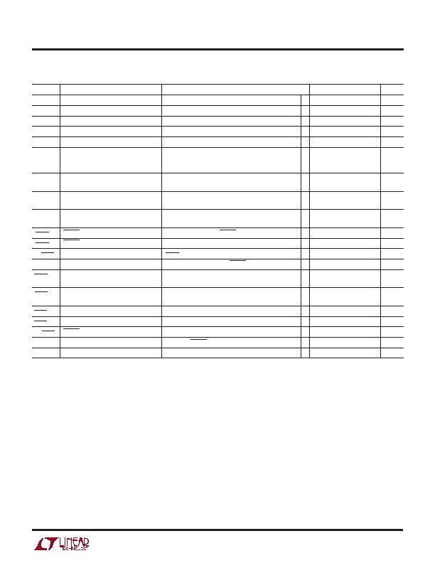
3
LTC4212
4212f
V
PGFHI
Power Good Glitch Filter High Threshold
q 1.20
1.236
1.26
V
V
PGFHST
Power Good Glitch Filter Hysterisis
(Note 4)
40
mV
V
PGTHI
Power Good Timer High Threshold
q 0.928
0.952 0.976
V
V
PGTLO
Power Good Timer Low Threshold
q 0.640
0.657 0.680
V
V
PGTV
Power Good Timer Delta Threshold
q 0.283
0.295 0.304
V
I
PGT
Power Good Timer Pin Current
Power Good Timer On, C
PGT
Charging, PGT = 0.65V
q 5.61
5.1 4.59
礎
Power Good Timer On, C
PGT
Discharging, PGT = 0.95V q 4.63
5.2
5.77
礎
Power Good Timer Off, PGT = 1.5V
5
mA
I
PGF
Power Good Glitch Filter Pin Current
Power Good Glitch Filter On, C
PGF
Charging
q 5.61
-5.1
4.49
礎
Power Good Timer Off, PGF = 1.5V
5
mA
I
TMR
TIMER Current
Timer On, V
TIMER
= 1V
q 2.5
2
1.5
礎
Timer Off, TIMER = 1.5V
5
mA
V
TMR
TIMER Threshold
TIMER Low to High
q 1.20
1.236
1.26
V
TIMER High to Low
q 0.15
0.200
0.40
V
V
FAULT
FAULT Threshold
Latched Off Threshold, FAULT High to Low
q 1.20
1.236
1.26
V
V
FAULTHST
FAULT Threshold Hysteresis
50
mV
V
OLFAULT
Output Low Voltage
I
FAULT
= 1.6mA
q
0.14
0.4
V
t
TO
Power Good Time-Out
C
PGT
=10nF, PGT = 0.1V to FAULT Low
q 16.3
18.16
20
ms
t
FAULTLO
Power Good Input Low at Time-Out to End of 14th PGT Cycle
1
祍
GATE Discharging
t
FAULTVG
Valid Power Good Glitch to GATE
PGF > 1.26V
1.5
祍
Discharging
t
FAULTFC
FAST COMP Trip to GATE Discharging V
CB
= 0mV to 200mV Step
q
500
700
ns
t
FAULTSC
SLOW COMP Trip to GATE Discharging V
CB
= 0mV to 100mV Step
q
10
18
30
祍
t
EXTFAULT
FAULT Low to GATE Discharging
V
FAULT
= 5V to 0V
q
1
3
5
祍
t
RESET
Circuit Breaker Reset Delay Time
ON Low to FAULT High
q
120
250
祍
t
OFF
Turn-Off Time
ON Low to GATE Off
10
祍
The q denotes specifications which apply over the full operating
temperature range, otherwise specifications are T
A
= 25?/SPAN>C. V
CC
= 5V, unless otherwise noted. (Note 2)
ELECTRICAL CHARACTERISTICS
Note 1: Absolute Maximum Ratings are those values beyond which the life
of a device may be impaired.
Note 2: All current into device pins are positive; all current out of device
pins are negative; all voltages are referenced to ground unless otherwise
specified.
Note 3: An internal clamp limits the GATE pin to a minimum of 10V above
V
CC
. Driving this pin to voltages beyond the clamp may damage the part. If
a lower GATE pin voltage is desired, use an external zener diode. The GATE
capacitance must be <0.15礔 at maximum V
CC
.
Note 4: Guaranteed by design and not tested in production.
SYMBOL
PARAMETER
CONDITIONS
MIN
TYP
MAX
UNITS
相关PDF资料 |
PDF描述 |
|---|---|
| LTC4214-1IMS#TRPBF | IC CTRLR HOTSWAP NEGVOLT 10MSOP |
| LTC4215IUFD#PBF | IC CNTRLR HOT SWAP 24-QFN |
| LTC4216IDE#TRPBF | IC CNTRLR HOT SWAP 12-DFN |
| LTC4221IGN#TRPBF | IC CTRLR HOTSWAP DUAL 16SSOP |
| LTC4222CG#PBF | IC CTRLR DUAL HOT SWAP 36-SSOP |
相关代理商/技术参数 |
参数描述 |
|---|---|
| LTC4213 | 制造商:LINER 制造商全称:Linear Technology 功能描述:No RSENSE? Electronic Circuit Breaker |
| LTC4213CDDB | 制造商:LINER 制造商全称:Linear Technology 功能描述:No RSENSE? Electronic Circuit Breaker |
| LTC4213CDDB#PBF | 制造商:Linear Technology 功能描述:Hot Swap Controller 1-CH 6V 8-Pin DFN EP 制造商:Linear Technology 功能描述:HOT SWAP CNTRL 6V INT SW 8DFN 制造商:Linear Technology 功能描述:HOT SWAP CNTRL, 6V, INT SW, 8DFN |
| LTC4213CDDB#TRMPBF | 功能描述:IC CIRC BREAK ELEC 8-DFN RoHS:是 类别:集成电路 (IC) >> 专用 IC 系列:* 产品培训模块:Lead (SnPb) Finish for COTS Obsolescence Mitigation Program 标准包装:1 系列:- 类型:调帧器 应用:数据传输 安装类型:表面贴装 封装/外壳:400-BBGA 供应商设备封装:400-PBGA(27x27) 包装:散装 |
| LTC4213CDDB#TRPBF | 功能描述:IC CIRC BREAK ELEC 8-DFN RoHS:是 类别:集成电路 (IC) >> 专用 IC 系列:* 产品培训模块:Lead (SnPb) Finish for COTS Obsolescence Mitigation Program 标准包装:1 系列:- 类型:调帧器 应用:数据传输 安装类型:表面贴装 封装/外壳:400-BBGA 供应商设备封装:400-PBGA(27x27) 包装:散装 |
发布紧急采购,3分钟左右您将得到回复。