参数资料
| 型号: | LTC4213IDDB#TRMPBF |
| 厂商: | Linear Technology |
| 文件页数: | 6/20页 |
| 文件大小: | 0K |
| 描述: | IC CIRC BREAK ELEC 8-DFN |
| 标准包装: | 1 |
| 系列: | * |
| 其它名称: | LTC4213IDDB#TRMPBFDKR |
LTC4213
14
4213f
Operating temperature of 0° to 70°C.
RDSON @ 25°C = 100%
RDSON @ 0°C = 90%
RDSON @ 70°C = 120%
MOSFET resistance variation:
RDSON(NOM) = 15m 0.82 = 12.3m
RDSON(MAX) = 15m 1.333 0.93 1.2 = 15m 1.488
= 22.3m
RDSON(MIN) = 15m 0.667 0.80 0.90 = 15m 0.480
= 7.2m
VCB variation:
NOM VCB = 25mV = 100%
MIN VCB = 22.5mV = 90%
MAX VCB = 27.5mV = 110%
The current limits are:
ILIMIT(NOM) = 25mV/12.3m = 2.03A
ILIMIT(MIN) = 22.5mV/22.3m = 1.01A
ILIMIT(MAX) = 27.5mV/7.2m = 3.82A
For proper operation, the minimum current limit must
exceed the circuit maximum operating load current with
margin. So this system is suitable for operating load
current up to 1A. From this calculation, we can start with
the general rule for MOSFET RDSON by assuming maxi-
mum operating load current is roughly half of the
ILIMIT(NOM). Equation 7 shows the rule of thumb.
I
V
R
OPMAX
CB NOM
DSON NOM
=
()
()
2
7
Note that the RDSON(NOM) is at the LTC4213 nominal
operating VGSMAX rather than at typical vendor spec.
Table 1 gives the nominal operating VGSMAX at the
various operating VCC. From this table users can refer to
the MOSFET’s data sheet to obtain the RDSON(NOM) value.
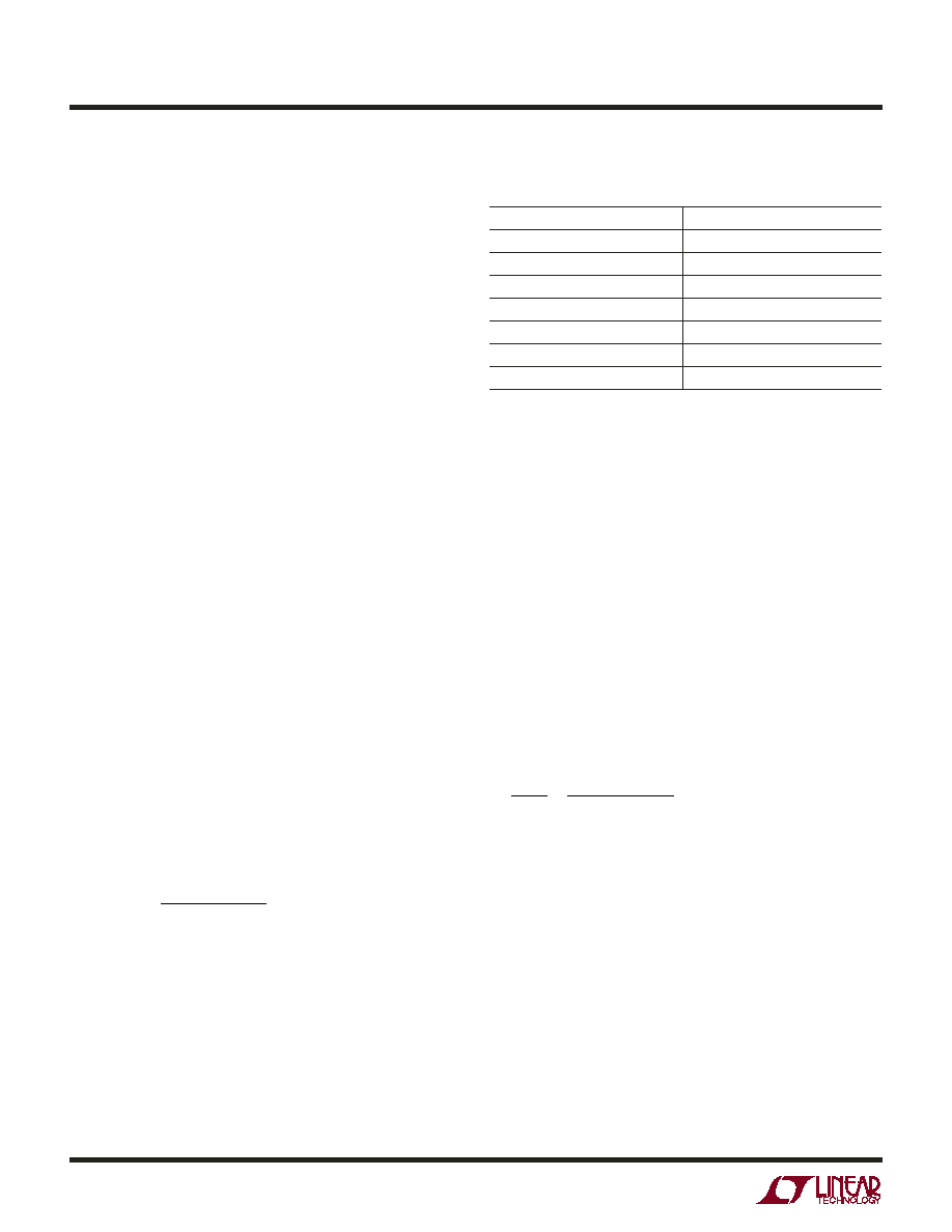
Table 1. Nominal Operating VGSMAX for Typical Bias
Supply Voltage
VCC (V)
VGSMAX (V)
2.3
4.3
2.5
5.0
2.7
5.6
3.0
6.5
3.3
7.0
5.0
7.0
6.0
7.0
Load Supply Power-Up after Circuit Breaker Armed
Figure 4 shows a normal power-up sequence for the
circuit in Figure 1 where the VIN load supply power-up after
circuit breaker is armed. VCC is first powered up by an
auxiliary bias supply. VCC rises above 2.07V at time
point 1. VON exceeds 0.8V at time point 2. After a 60s
debounce delay, the GATE pin starts ramping up at time
point 3. The external MOSFET starts conducting at time
point 4. At time point 5, VGATE exceed VGSARM and the
circuit breaker is armed. After 50s (tREADY delay), READY
pulls high by an external resistor at time point 6. READY
signals the VIN load supply module to start its ramp. The
load supply begins soft-start ramp at time point 7. The load
supply ramp rate must be slow to prevent circuit breaker
tripping as in equation (8).
V
t
II
C
IN
OPMAX
LOAD
<
()
8
Where IOPMAX is the maximum operating current defined
by equation 7.
For illustration, VCB = 25mV and RDSON = 3.5m at the
nominal operating VGSMAX. The maximum operating
current is 3.5A (refer to equation 7). Assuming the load
can draw a current of 2A at power-up, there is a margin of
1.5A available for CLOAD of 100F and VIN ramp rate should
be <15V/ms. At time point 8, the current through the
MOSFET reduces after CLOAD is fully charged.
APPLICATIO S I FOR ATIO
WU
U
相关PDF资料 |
PDF描述 |
|---|---|
| LFEC6E-4FN256C | IC FPGA 6.1KLUTS 195I/O 256-BGA |
| ABB35DHAT | CONN EDGECARD 70POS R/A .050 SLD |
| AMM18DTMI-S189 | CONN EDGECARD 36POS R/A .156 SLD |
| AMM18DTBI-S189 | CONN EDGECARD 36POS R/A .156 SLD |
| AMM18DTAI-S189 | CONN EDGECARD 36POS R/A .156 SLD |
相关代理商/技术参数 |
参数描述 |
|---|---|
| LTC4214 | 制造商:LINER 制造商全称:Linear Technology 功能描述:Dual Hot Swap Controller |
| LTC4214-1 | 制造商:LINER 制造商全称:Linear Technology 功能描述:Negative Low Voltage Hot Swap Controllers |
| LTC4214-1CMS | 功能描述:IC CTRLR HOTSWAP NEGVOLT 10MSOP RoHS:否 类别:集成电路 (IC) >> PMIC - 热交换 系列:- 标准包装:50 系列:- 类型:热交换控制器 应用:-48V 远程电力系统,AdvancedTCA ? 系统,高可用性 内部开关:无 电流限制:可调 电源电压:11.5 V ~ 14.5 V 工作温度:-40°C ~ 85°C 安装类型:表面贴装 封装/外壳:10-TFSOP,10-MSOP(0.118",3.00mm 宽) 供应商设备封装:10-MSOP 包装:管件 |
| LTC4214-1CMS#PBF | 功能描述:IC CTRLR HOTSWAP NEGVOLT 10MSOP RoHS:是 类别:集成电路 (IC) >> PMIC - 热交换 系列:- 标准包装:50 系列:- 类型:热交换控制器 应用:-48V 远程电力系统,AdvancedTCA ? 系统,高可用性 内部开关:无 电流限制:可调 电源电压:11.5 V ~ 14.5 V 工作温度:-40°C ~ 85°C 安装类型:表面贴装 封装/外壳:10-TFSOP,10-MSOP(0.118",3.00mm 宽) 供应商设备封装:10-MSOP 包装:管件 |
| LTC4214-1CMS#TR | 功能描述:IC CTRLR HOTSWAP NEG LV 10MSOP RoHS:否 类别:集成电路 (IC) >> PMIC - 热交换 系列:- 标准包装:50 系列:- 类型:热交换控制器 应用:-48V 远程电力系统,AdvancedTCA ? 系统,高可用性 内部开关:无 电流限制:可调 电源电压:11.5 V ~ 14.5 V 工作温度:-40°C ~ 85°C 安装类型:表面贴装 封装/外壳:10-TFSOP,10-MSOP(0.118",3.00mm 宽) 供应商设备封装:10-MSOP 包装:管件 |
发布紧急采购,3分钟左右您将得到回复。