- 您现在的位置:买卖IC网 > Datasheet目录42 > LTC4216IDE#TRPBF (Linear Technology)IC CNTRLR HOT SWAP 12-DFN Datasheet资料下载
参数资料
| 型号: | LTC4216IDE#TRPBF |
| 厂商: | Linear Technology |
| 文件页数: | 10/26页 |
| 文件大小: | 311K |
| 描述: | IC CNTRLR HOT SWAP 12-DFN |
| 标准包装: | 2,500 |
| 类型: | 热交换控制器 |
| 应用: | 通用 |
| 内部开关: | 无 |
| 电源电压: | 2.3 V ~ 6 V |
| 工作温度: | -40°C ~ 85°C |
| 安装类型: | 表面贴装 |
| 封装/外壳: | 12-WFDFN 裸露焊盘 |
| 供应商设备封装: | 12-DFN(4x3) |
| 包装: | 带卷 (TR) |
LTC4216
10
4216fa
For more information www.linear.com/LTC4216
applicaTions inForMaTion
switch when the TIMER pin voltage exceeds its threshold.
The timer period for C1 to charge up to the TIMER pin
threshold, V
TMR(TH)
(1.253V), is given by:
t
V C
A
TIMER
=
1 253
1
2
.
"
(1)
For example, if C1 = 10nF, t
TIMER
= 6.2ms.
FB Glitch Filtering
The FB pin is used to monitor the output voltage of the
external MOSFET through a resistive divider. Any tran-
sients on the FB pin due to the output low spikes will
pull RESET low. To prevent RESET from generating an
unwanted system reset, the FB comparator has a glitch
filter to ride out these glitches. The filter time is 20祍 for
large transients (greater than 150mV) and up to 100祍
for small transients. The relationship between glitch filter
time and the FB pin transient voltage or FB overdrive is
shown in Figure 1.
FB pin voltage rises above 0.6V, the FB comparator output
goes low and a new timing cycle starts. After a complete
timing cycle at time point 6, RESET is pulled high by the
external pull-up resistor, R5. The timer period given by
Equation (1) sets the power-good delay for RESET going
high. If the FB pin voltage stays above 0.6V for less than
a timing cycle at time point 4, the RESET output remains
low. Any overcurrent fault detected by the electronic cir-
cuit breaker or FAULT pin driven low externally during the
timing cycle, will also pull the TIMER pin low and RESET
output remains low.
When the device enters an undervoltage lockout condition
or the ON pin voltage drops below 0.4V, RESET is pulled
low, ignoring the FB pin voltage.
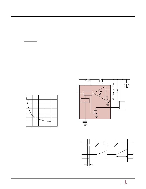
Figure 2. Output Voltage Monitor Block Diagram
Figure 3. Output Voltage Monitor
Waveforms in Normal Operation
Output Voltage Monitor
As shown in Figure 2, the output voltage is monitored
through a resistive divider, R3 and R4, connected at the
FB pin, and a FB comparator with 0.6V threshold.
The normal operation of the output voltage monitor after a
start-up cycle is shown in Figure 3. At time point 1, when the
FB pin voltage falls below 0.6V, the FB comparator output
goes high. RESET is pulled low by an internal N-channel
switch after a glitch filter delay at time point 2. When the
Figure 1. FB Comparator Glitch Filter Time vs FB Overdrive
FB OVERDRIVE (mV)
0
100
120
140
160
120
4216 F01
80
60
40
80
200
40
20
0
T
A
= 25癈
LOGIC
TIMER
TIMER
LTC4216**
SENSEP
0.6V
V
CC
V
IN
ON
FB
R4
R3
R
SENSE
R5
M2
M1
RESET
SENSEN
GATE
+
C1
C
LOAD
**ADDITIONAL DETAILS
OMITTED FOR CLARITY
RESET
礟
V
OUT
+
4216 F02
1 2
V
OUT
V
TMR(TH)
V
FB
< 0.6V
V
FB
> 0.6V
V
FB
< 0.6V V
FB
> 0.6V
TIMER
RESET
GLITCH FILTER DELAY
3
4
5
6
POWER-GOOD
DELAY
2礎
2礎
4216 F03
相关PDF资料 |
PDF描述 |
|---|---|
| LTC4221IGN#TRPBF | IC CTRLR HOTSWAP DUAL 16SSOP |
| LTC4222CG#PBF | IC CTRLR DUAL HOT SWAP 36-SSOP |
| LTC4223CDHD-2#PBF | IC CNTRLR HOT SWAP DUAL 16-DFN |
| LTC4224IDDB-2#TRPBF | IC CNTRLR HOT SWAP DUAL 10-DFN |
| LTC4225IGN-1#PBF | IC CONTROLLER HOT SWAP 24-SSOP |
相关代理商/技术参数 |
参数描述 |
|---|---|
| LTC4216IMS | 制造商:LINER 制造商全称:Linear Technology 功能描述:Ultralow Voltage Hot Swap Controller |
| LTC4216IMS#PBF | 功能描述:IC CNTRLR HOT SWAP 10-MSOP RoHS:是 类别:集成电路 (IC) >> PMIC - 热交换 系列:- 标准包装:50 系列:- 类型:热交换控制器 应用:-48V 远程电力系统,AdvancedTCA ? 系统,高可用性 内部开关:无 电流限制:可调 电源电压:11.5 V ~ 14.5 V 工作温度:-40°C ~ 85°C 安装类型:表面贴装 封装/外壳:10-TFSOP,10-MSOP(0.118",3.00mm 宽) 供应商设备封装:10-MSOP 包装:管件 |
| LTC4216IMS#TRPBF | 功能描述:IC CNTRLR HOT SWAP 10-MSOP RoHS:是 类别:集成电路 (IC) >> PMIC - 热交换 系列:- 标准包装:50 系列:- 类型:热交换控制器 应用:-48V 远程电力系统,AdvancedTCA ? 系统,高可用性 内部开关:无 电流限制:可调 电源电压:11.5 V ~ 14.5 V 工作温度:-40°C ~ 85°C 安装类型:表面贴装 封装/外壳:10-TFSOP,10-MSOP(0.118",3.00mm 宽) 供应商设备封装:10-MSOP 包装:管件 |
| LTC4217 | 制造商:LINER 制造商全称:Linear Technology 功能描述:2A Integrated Hot Swap Controller |
| LTC4217CDHC | 制造商:LINER 制造商全称:Linear Technology 功能描述:2A Integrated Hot Swap Controller |
发布紧急采购,3分钟左右您将得到回复。