- 您现在的位置:买卖IC网 > PDF目录79699 > LTC4217IFE#TRPBF (LINEAR TECHNOLOGY CORP) 1-CHANNEL POWER SUPPLY MANAGEMENT CKT, PDSO20 PDF资料下载
参数资料
| 型号: | LTC4217IFE#TRPBF |
| 厂商: | LINEAR TECHNOLOGY CORP |
| 元件分类: | 电源管理 |
| 英文描述: | 1-CHANNEL POWER SUPPLY MANAGEMENT CKT, PDSO20 |
| 封装: | 4.40 MM, LEAD FREE, PLASTIC, SSOP-20 |
| 文件页数: | 6/18页 |
| 文件大小: | 238K |
| 代理商: | LTC4217IFE#TRPBF |
LTC4217
14
4217fe
applicaTions inForMaTion
invoked by tying the TIMER pin to INTVCC. After the 2ms
timeout the FLT pin needs to pull-down on the UV pin to
restart the power-up sequence.
Since the default values for overvoltage, undervoltage and
power good thresholds for the 12V fixed version match
the requirements, no external components are required
for the UV, OV and FB pins.
The final schematic in Figure 6 results in very few external
components. The pull-up resistor, R1, connects to the
PG pin while the 20k (R2) converts the IMON current to a
voltage at a ratio:
VIMON = 50[A/A] 20k IOUT = 1[V/A] IOUT
In addition there is a 0.1F bypass (C1) on the INTVCC pin.
Layout Considerations
In Hot Swap applications where load currents can be 2A,
narrowPCBtracksexhibitmoreresistancethanwidertracks
and operate at elevated temperatures. The minimum trace
width for 1oz copper foil is 0.02" per amp to make sure
the trace stays at a reasonable temperature. Using 0.03"
per amp or wider is recommended. Note that 1oz copper
exhibits a sheet resistance of about 0.5mΩ/square. Small
resistances add up quickly in high current applications.
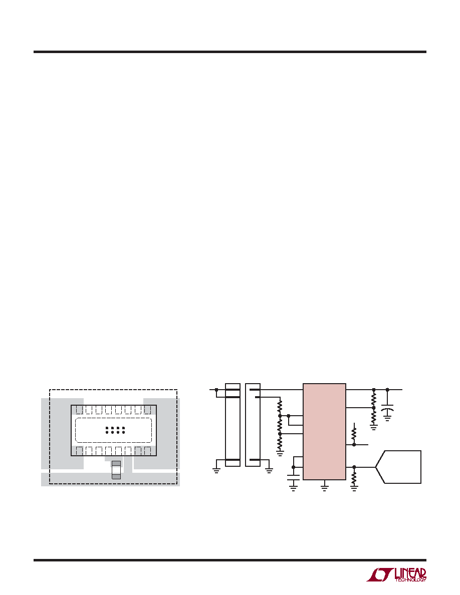
There are two VDD pins on opposite sides of the package
that connect to the sense resistor and MOSFET. The PCB
layout should be balanced and symmetrical to each VDD
pin to balance current in the MOSFET bond wires. Figure 7
shows a recommended layout for the LTC4217.
Although the MOSFET is self protected from overtem-
perature, it is recommended to solder the backside of the
package to a copper trace to provide a good heat sink. Note
that the backside is connected to the SENSE pin and can-
not be soldered to the ground plane. During normal loads
the power dissipated in the MOSFET is as high as 0.23W.
A 10mm × 10mm area of 1oz copper should be sufficient.
This area of copper can be divided in many layers.
It is also important to put C1, the bypass capacitor for
the INTVCC pin as close as possible between the INTVCC
and GND.
Additional Applications
TheLTC4217hasawideoperatingrangefrom2.9Vto26.5V.
The UV, OV and PG thresholds are set with few resistors.
All other functions are independent of supply voltage.
Figure 8 shows a 3.3V application with a UV threshold of
2.87V, an OV threshold of 3.77V and a PG threshold of
3.05V. The last page includes a 24V application with a UV
threshold of 19.9V, an OV threshold of 26.3V and a PG
threshold of 20.75V.
Figure 8. 3.3V, 1.5A Card Resident Application
R4
14.7k
R5
10k
R1
17.4k
ADC
R2
3.16k
CT
0.1F
R3
10k
3.3V
RMON
20k
4217 F08
R6
10k
CL
100F
VDD
UV
OUT
FB
PG
GND
IMON
LTC4217FE
OV
INTVCC
TIMER
FLT
+
VOUT
3.3V
1.5A
4217 F07
HEAT SINK
VIA TO
SINK
GND
C
OUT
VDD
Figure 7. Recommended Layout
相关PDF资料 |
PDF描述 |
|---|---|
| LX1431CDMT | 1-OUTPUT TWO TERM VOLTAGE REFERENCE, 5 V, PDSO8 |
| LKP5660-5ERDDTB1 | 2-OUTPUT 250 W AC-DC PWR FACTOR CORR MODULE |
| LES020ZG-3N2N1H | 1-OUTPUT 15 W DC-DC REG PWR SUPPLY MODULE |
| LES020ZG-3N2N | 1-OUTPUT 15 W DC-DC REG PWR SUPPLY MODULE |
| LES020ZG-3N3N9 | 1-OUTPUT 15 W DC-DC REG PWR SUPPLY MODULE |
相关代理商/技术参数 |
参数描述 |
|---|---|
| LTC4218 | 制造商:LINER 制造商全称:Linear Technology 功能描述:Dual Hot Swap Controller |
| LTC4218CDHC-12#PBF | 功能描述:IC CTLR HOT SWAP 16-DFN RoHS:是 类别:集成电路 (IC) >> PMIC - 热交换 系列:- 产品培训模块:Obsolescence Mitigation Program 标准包装:100 系列:- 类型:热插拔开关 应用:通用 内部开关:是 电流限制:可调 电源电压:9 V ~ 13.2 V 工作温度:-40°C ~ 150°C 安装类型:表面贴装 封装/外壳:10-WFDFN 裸露焊盘 供应商设备封装:10-TDFN-EP(3x3) 包装:管件 |
| LTC4218CDHC-12#TRPBF | 功能描述:IC CNTRLR HOT SWAP 16-DFN RoHS:是 类别:集成电路 (IC) >> PMIC - 热交换 系列:- 产品培训模块:Obsolescence Mitigation Program 标准包装:100 系列:- 类型:热插拔开关 应用:通用 内部开关:是 电流限制:可调 电源电压:9 V ~ 13.2 V 工作温度:-40°C ~ 150°C 安装类型:表面贴装 封装/外壳:10-WFDFN 裸露焊盘 供应商设备封装:10-TDFN-EP(3x3) 包装:管件 |
| LTC4218CDHC-12-PBF | 制造商:LINER 制造商全称:Linear Technology 功能描述:Hot Swap Controller |
| LTC4218CDHC-12-TRPBF | 制造商:LINER 制造商全称:Linear Technology 功能描述:Hot Swap Controller |
发布紧急采购,3分钟左右您将得到回复。