- 您现在的位置:买卖IC网 > PDF目录30772 > LTC4219IDHC-5#PBF (LINEAR TECHNOLOGY CORP) 1-CHANNEL POWER SUPPLY SUPPORT CKT, PDSO16 PDF资料下载
参数资料
| 型号: | LTC4219IDHC-5#PBF |
| 厂商: | LINEAR TECHNOLOGY CORP |
| 元件分类: | 电源管理 |
| 英文描述: | 1-CHANNEL POWER SUPPLY SUPPORT CKT, PDSO16 |
| 封装: | 5 X 3 MM, LEAD FREE, PLASTIC, MO-229WJED-1, DFN-16 |
| 文件页数: | 3/18页 |
| 文件大小: | 195K |
| 代理商: | LTC4219IDHC-5#PBF |
LTC4219
11
4219fb
APPLICATIONS INFORMATION
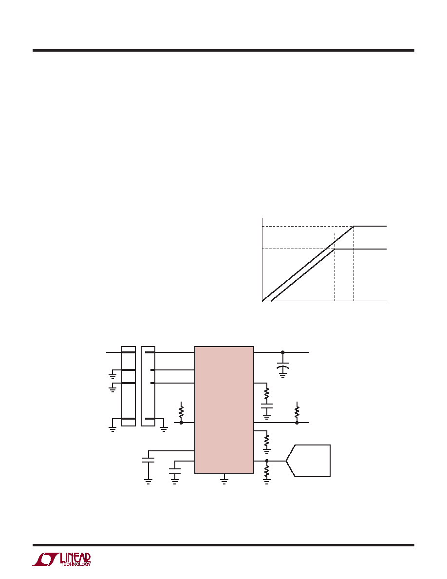
versus time (Figure 2). The voltage at the GATE pin rises
with a slope of 0.3V/ms and the supply inrush current is
set at:
IINRUSH = CL (0.3V/ms)
This gate slope is designed to charge up a 1000μF capacitor
to 12V in 40ms, with an inrush current of 300mA. This
allows the inrush current to stay under the current limit
threshold (1.5A) for capacitors less than 1000μF. Included
in the Typical Performance Characteristics section is a
graph of the Safe Operating Area for the MOSFET. It is
evident from this graph that the power dissipation at 12V,
300mA for 40ms is in the safe region.
Figure 2. Supply Turn-On
Figure 1. 2A, 12V Card Resident Application
The typical LTC4219 application is in a high availability
system that uses a positive voltage supply to distribute
power to individual cards. A complete application circuit
is shown in Figure 1. External component selection is
discussed in detail in the following sections.
Turn-On Sequence
Several conditions must be present before the internal
pass MOSFET can be turned on. First the supply VDD must
exceed its undervoltage lockout level. Next the internally
generated supply INTVCC must cross its 2.65V under-
voltage threshold. This generates a 25μs power-on-reset
pulse which clears the fault register and initializes internal
latches. Finally, the enable inputs EN1 and EN2 both must
be below the 1.15V threshold. All of these conditions must
be satised for the duration of 100ms to ensure that any
contact bounce during the insertion has ended.
The MOSFET is turned on by charging up the GATE with
a charge pump generated current source whose value is
adjusted by shunting a portion of the pull-up current to
ground. The charging current is controlled by the INRUSH
circuit that maintains a constant slope of GATE voltage
t1
t2
SLOPE = 0.3V/ms
GATE
OUT
VDD + 6.15
VDD
4219 F02
ADC
C1
0.1μF
12V
4219 F01
R4
10k
12V
R1
10k
CT
0.1μF
CL
330μF
VOUT
12V
2A
VDD
EN1
OUT
PG
GND
IMON
RSET
20k
RMON
20k
ISET
CGATE
0.1μF
RGATE
1k
GATE
LTC4219DHC-12
EN2
INTVCC
TIMER
FLT
+
相关PDF资料 |
PDF描述 |
|---|---|
| LTC4219CDHC-5#PBF | 1-CHANNEL POWER SUPPLY SUPPORT CKT, PDSO16 |
| LTC4224CMS-1#PBF | 2-CHANNEL POWER SUPPLY SUPPORT CKT, PDSO10 |
| LTC4224CDDB-2#PBF | 2-CHANNEL POWER SUPPLY SUPPORT CKT, PDSO10 |
| LTC4224IDDB-2#PBF | 2-CHANNEL POWER SUPPLY SUPPORT CKT, PDSO10 |
| LTC4224CDDB-1#TRPBF | 2-CHANNEL POWER SUPPLY SUPPORT CKT, PDSO10 |
相关代理商/技术参数 |
参数描述 |
|---|---|
| LTC4219IDHC-5-TRPBF | 制造商:LINER 制造商全称:Linear Technology 功能描述:5A Integrated Hot Swap Controller |
| LTC4220 | 制造商:LINER 制造商全称:Linear Technology 功能描述:Negative Voltage Hot Swap Controllers |
| LTC4221 | 制造商:LINER 制造商全称:Linear Technology 功能描述:Dual Hot Swap Controller/ Power Sequencer with Dual Speed, Dual Level Fault Protection |
| LTC4221CGN | 功能描述:IC CTRLR HOTSWAP DUAL 16SSOP RoHS:否 类别:集成电路 (IC) >> PMIC - 热交换 系列:- 产品培训模块:Obsolescence Mitigation Program 标准包装:100 系列:- 类型:热插拔开关 应用:通用 内部开关:是 电流限制:可调 电源电压:9 V ~ 13.2 V 工作温度:-40°C ~ 150°C 安装类型:表面贴装 封装/外壳:10-WFDFN 裸露焊盘 供应商设备封装:10-TDFN-EP(3x3) 包装:管件 |
| LTC4221CGN#PBF | 功能描述:IC CTLR HOT SWAP DUAL 16SSOP RoHS:是 类别:集成电路 (IC) >> PMIC - 热交换 系列:- 产品培训模块:Obsolescence Mitigation Program 标准包装:100 系列:- 类型:热插拔开关 应用:通用 内部开关:是 电流限制:可调 电源电压:9 V ~ 13.2 V 工作温度:-40°C ~ 150°C 安装类型:表面贴装 封装/外壳:10-WFDFN 裸露焊盘 供应商设备封装:10-TDFN-EP(3x3) 包装:管件 |
发布紧急采购,3分钟左右您将得到回复。