- 您现在的位置:买卖IC网 > Datasheet目录42 > LTC4223CDHD-2#PBF (Linear Technology)IC CNTRLR HOT SWAP DUAL 16-DFN Datasheet资料下载
参数资料
| 型号: | LTC4223CDHD-2#PBF |
| 厂商: | Linear Technology |
| 文件页数: | 4/24页 |
| 文件大小: | 290K |
| 描述: | IC CNTRLR HOT SWAP DUAL 16-DFN |
| 标准包装: | 73 |
| 类型: | 热交换控制器 |
| 应用: | ATCA,MicroTCA? |
| 内部开关: | 无 |
| 电源电压: | 2.7 V ~ 6 V |
| 工作温度: | 0°C ~ 70°C |
| 安装类型: | 表面贴装 |
| 封装/外壳: | 16-WFDFN 裸露焊盘 |
| 供应商设备封装: | 16-DFN(5x4) |
| 包装: | 管件 |
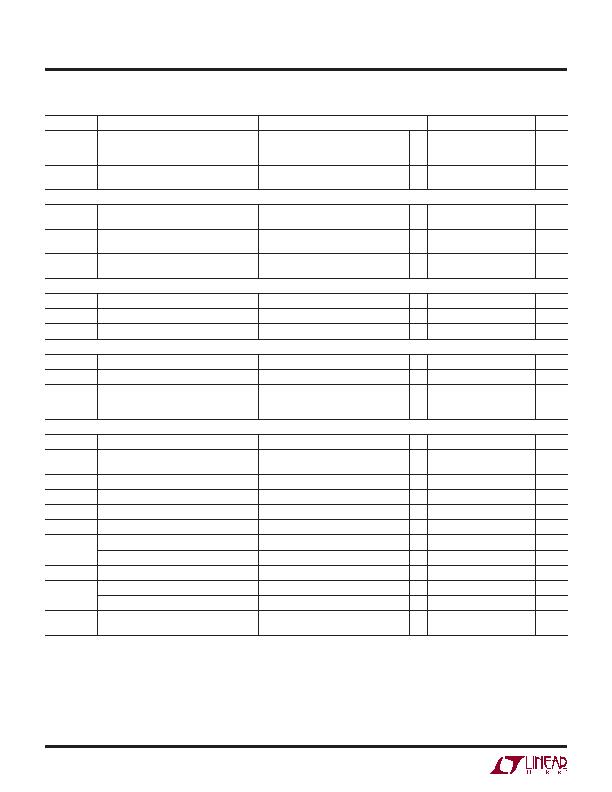
LTC4223-1/LTC4223-2
4
422312f
SYMBOL
PARAMETER
CONDITIONS
MIN
TYP
MAX
UNITS
I
TMR(UP)
TIMER Pull-Up Current
V
TIMER
= 1V, Initial Timing Cycle
V
TIMER
= 0V, In AUX Fault Mode
V
TIMER
= 0V, In 12V Fault Mode
?/DIV>
?/DIV>
?/DIV>
7
7
140
10
10
200
13
13
260
糀
糀
糀
I
TMR(DN)
TIMER Pull-Down Current
V
TIMER
= 2V, No Faults
V
TIMER
= 2V, In Reset Mode
?/DIV>
?/DIV>
1.3
2
2
8
2.6
16
糀
mA
Open Drain Outputs
V
OL
Output Low Voltage (
?/DIV>
F
?/DIV>
A
?/DIV>
U
?/DIV>
L
?/DIV>
T,
?/DIV>
1
?/DIV>
2
?/DIV>
P
?/DIV>
G
?/DIV>
O
?/DIV>
O
?/DIV>
D,
?/DIV>
A
?/DIV>
U
?/DIV>
X
?/DIV>
P
?/DIV>
G
?/DIV>
O
?/DIV>
O
?/DIV>
D)
I
OL
= 3mA
?/DIV>
0.15
0.4
V
V
OH
Output High Voltage (
?/DIV>
F
?/DIV>
A
?/DIV>
U
?/DIV>
L
?/DIV>
T,
?/DIV>
1
?/DIV>
2
?/DIV>
P
?/DIV>
G
?/DIV>
O
?/DIV>
O
?/DIV>
D,
?/DIV>
A
?/DIV>
U
?/DIV>
X
?/DIV>
P
?/DIV>
G
?/DIV>
O
?/DIV>
O
?/DIV>
D)
(Note 5)
?SPAN class="pst LTC4223CDHD-2-PBF_2351537_4"> V
CC
1
V
I
PU
Output Pin Pull-Up Current (
?/DIV>
F
?/DIV>
A
?/DIV>
U
?/DIV>
L
?/DIV>
T,
?/DIV>
1
?/DIV>
2
?/DIV>
P
?/DIV>
G
?/DIV>
O
?/DIV>
O
?/DIV>
D,
?/DIV>
A
?/DIV>
U
?/DIV>
X
?/DIV>
P
?/DIV>
G
?/DIV>
O
?/DIV>
O
?/DIV>
D)
V
PU
= 1.5V
?/DIV>
6
10
14
糀
Logic Inputs
V
IN(TH)
Logic Input Threshold (12ON, AUXON,
?/DIV>
E
?/DIV>
N)
?/DIV>
0.8
2
V
I
IN(LEAK)
Input Leakage Current (12ON, AUXON)
V
IN
= V
CC
?/DIV>
?
糀
R
PU
?/DIV>
E
?/DIV>
N Pin Pull-Up Resistance
?/DIV>
60
100
140
k?/DIV>
Other Pin Functions
I
12VSENSE
12V
SENSE
Pin Input Current
V
12VSENSE
= 12V
?/DIV>
10
50
100
糀
I
12VOUT
12V
OUT
Pin Input Current
Gate Drive On, V
12VOUT
= 12V
?/DIV>
20
50
100
糀
R
OUT(DIS)
OUT Pin Discharge Resistance
12V
OUT
AUXOUT
Gate Drive Off
V
12VOUT
= 6V
V
AUXVOUT
= 2V
?/DIV>
?/DIV>
400
375
800
750
1600
1500
?/DIV>
?/DIV>
Propagation Delays
t
CB
AUX Circuit Breaker Trip Delay
After Power Up
?/DIV>
12
25
50
約
t
PHL(SENSE)
Sense Voltage, (12V
IN
12V
SENSE
)
High to 12V
GATE
Low
擵
SENSE
= 300mV, C
12VGATE
= 10nF
擵
SENSE
= 100mV, C
12VGATE
= 10nF
?/DIV>
?/DIV>
0.5
5
1
12
約
約
t
PHH(AUXON)
AUXON High to AUXOUT High
?/DIV>
15
30
約
t
PHH(12ON)
12ON High to 12V
GATE
High
?/DIV>
30
60
約
t
RST(ON)
Input Low (12ON, AUXON) to
?/DIV>
F
?/DIV>
A
?/DIV>
U
?/DIV>
L
?/DIV>
T High
?/DIV>
20
40
約
t
RST(VCC)
V
CC
Low to
?/DIV>
F
?/DIV>
A
?/DIV>
U
?/DIV>
L
?/DIV>
T High
?/DIV>
80
150
約
t
PLL(UVLO)
12V
IN
Low to 12V
GATE
Low
?/DIV>
6
12
18
約
AUXIN Low to
?/DIV>
A
?/DIV>
U
?/DIV>
X
?/DIV>
P
?/DIV>
G
?/DIV>
O
?/DIV>
O
?/DIV>
D High
?/DIV>
6
12
18
約
t
PHL(GATE)
?/DIV>
E
?/DIV>
N High to 12V
GATE
Low
?/DIV>
20
40
約
t
PLH(PG)
12V
OUT
Low to
?/DIV>
1
?/DIV>
2
?/DIV>
P
?/DIV>
G
?/DIV>
O
?/DIV>
O
?/DIV>
D High
?/DIV>
20
40
約
AUXOUT Low to
?/DIV>
A
?/DIV>
U
?/DIV>
X
?/DIV>
P
?/DIV>
G
?/DIV>
O
?/DIV>
O
?/DIV>
D High
?/DIV>
20
40
約
t
P(12IMON)
Input Sense Voltage Step to 12IMON
Propagation Delay
擵
SENSE
= 100mV
?/DIV>
2
6
約
Note 1: Stresses beyond those listed under Absolute Maximum Ratings
may cause permanent damage to the device. Exposure to any Absolute
Maximum Rating condition for extended periods may affect device
reliability and lifetime.
Note 2: All currents into device pins are positive; all currents out of
the device pins are negative. All voltages are referenced to GND unless
otherwise speci ed.
Note 3: An internal clamp limits the 12V
GATE
pin to a minimum of 4.5V
above 12V
OUT
. Driving this pin to voltages beyond the clamp may damage
the device.
Note 4: For the DFN package, the AUX switch on resistance, R
DS(ON)
limit
is guaranteed by correlation to wafer test measurements.
Note 5: The output pins
?/DIV>
F
?/DIV>
A
?/DIV>
U
?/DIV>
L
?/DIV>
T,
?/DIV>
1
?/DIV>
2
?/DIV>
P
?/DIV>
G
?/DIV>
O
?/DIV>
O
?/DIV>
D and
?/DIV>
A
?/DIV>
U
?/DIV>
X
?/DIV>
P
?/DIV>
G
?/DIV>
O
?/DIV>
O
?/DIV>
D have an internal
pull-up to V
CC
of 10糀. However, an external pull-up resistor may be used
when faster rise time is required or for V
OH
voltages greater than V
CC
.
ELECTRICAL CHARACTERISTICS
The ?/SPAN> denotes the speci cations which apply over the full operating
temperature range, otherwise speci cations are T
A
= 25癈, V
CC
= 3.3V, V
AUXIN
= 3.3V, V
12VIN
=12V, unless otherwise speci ed. (Note 2)
相关PDF资料 |
PDF描述 |
|---|---|
| LTC4224IDDB-2#TRPBF | IC CNTRLR HOT SWAP DUAL 10-DFN |
| LTC4225IGN-1#PBF | IC CONTROLLER HOT SWAP 24-SSOP |
| LTC4230CGN#TRPBF | IC CONTRLLR HOT SWAP TRPL 20SSOP |
| LTC4232CDHC#TRPBF | IC CTLR HOT SWAP 5A 16-DFN |
| LTC4240IGN#TRPBF | IC CTRLR HOTSWAP CPCI I2C 28SSOP |
相关代理商/技术参数 |
参数描述 |
|---|---|
| LTC4223CDHD-2TRPBF | 制造商:LINER 制造商全称:Linear Technology 功能描述:Dual Supply Hot Swap Controller for Advanced Mezzanine Card |
| LTC4223CGN-1#PBF | 功能描述:IC CNTRLR HOT SWAP DUAL 16-SSOP RoHS:是 类别:集成电路 (IC) >> PMIC - 热交换 系列:- 标准包装:50 系列:- 类型:热交换控制器 应用:-48V 远程电力系统,AdvancedTCA ? 系统,高可用性 内部开关:无 电流限制:可调 电源电压:11.5 V ~ 14.5 V 工作温度:-40°C ~ 85°C 安装类型:表面贴装 封装/外壳:10-TFSOP,10-MSOP(0.118",3.00mm 宽) 供应商设备封装:10-MSOP 包装:管件 |
| LTC4223CGN-1#TRPBF | 功能描述:IC CNTRLR HOT SWAP DUAL 16-SSOP RoHS:是 类别:集成电路 (IC) >> PMIC - 热交换 系列:- 标准包装:50 系列:- 类型:热交换控制器 应用:-48V 远程电力系统,AdvancedTCA ? 系统,高可用性 内部开关:无 电流限制:可调 电源电压:11.5 V ~ 14.5 V 工作温度:-40°C ~ 85°C 安装类型:表面贴装 封装/外壳:10-TFSOP,10-MSOP(0.118",3.00mm 宽) 供应商设备封装:10-MSOP 包装:管件 |
| LTC4223CGN-1PBF | 制造商:LINER 制造商全称:Linear Technology 功能描述:Dual Supply Hot Swap Controller for Advanced Mezzanine Card |
| LTC4223CGN-1TRPBF | 制造商:LINER 制造商全称:Linear Technology 功能描述:Dual Supply Hot Swap Controller for Advanced Mezzanine Card |
发布紧急采购,3分钟左右您将得到回复。