- 您现在的位置:买卖IC网 > PDF目录22109 > LTC4261IGN#TR (Linear Technology)IC CTRLR HOTSWAP W/ADC 28-SSOP PDF资料下载
参数资料
| 型号: | LTC4261IGN#TR |
| 厂商: | Linear Technology |
| 文件页数: | 20/34页 |
| 文件大小: | 361K |
| 描述: | IC CTRLR HOTSWAP W/ADC 28-SSOP |
| 标准包装: | 2,500 |
| 类型: | 热交换控制器 |
| 应用: | 通用 |
| 内部开关: | 无 |
| 电源电压: | 9 V ~ 11.2 V |
| 工作温度: | -40°C ~ 85°C |
| 安装类型: | 表面贴装 |
| 封装/外壳: | 28-SSOP(0.154",3.90mm 宽) |
| 供应商设备封装: | 28-SSOP |
| 包装: | 带卷 (TR) |
第1页第2页第3页第4页第5页第6页第7页第8页第9页第10页第11页第12页第13页第14页第15页第16页第17页第18页第19页当前第20页第21页第22页第23页第24页第25页第26页第27页第28页第29页第30页第31页第32页第33页第34页
LTC4261/LTC4261-2
20
42612fc
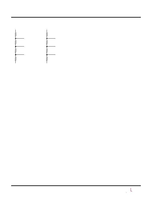
Figure 8. Adjustment of Undervoltage Thresholds
for Larger (8a) or Smaller (8b) Hysteresis
present bit A1 and the undervoltage fault bit B1. The
power good signals at PG and PGIO are also reset.
The undervoltage present bit A1 is cleared when the
UVH pin rises above 2.56V and the UVL pin rises above
2.291V + dV
UV
. After a delay of t
D
, the FET will turn on
again unless the undervoltage auto-retry has been dis-
abled by clearing bit D1.
When power is applied to the device, if UVL is below
the 2.291V threshold and UVH is below 2.56V dV
UV
after INTV
CC
crosses its undervoltage lock out threshold
(4.25V), an undervoltage fault will be logged in the fault
register.
Because of the compromises of selecting from a table of
discrete resistor values (1% resistors in 2% increments,
0.1% resistors in 1% increments), best possible OV and
UV accuracy is achieved using separate dividers for each
pin. This increases the total number of resistors from
three or four to as many as six, but maximizes accuracy,
greatly simplifies calculations and facilitates running
changes to accommodate multiple standards or custom-
ization without any board changes.
FET Short Fault
A FET short fault will be reported if the data converter mea-
sures a current sense voltage greater than or equal to 2mV
while the FET is turned off. This condition sets the FET
short present bit A5 and the FET short fault bit B5.
Power Bad Fault
After the FET is turned on and the power good outputs
pull PG and PGIO low, a delay timer with duration of 4t
D
is
started and the level of the PGI pin is checked (Figure 3).
If the PGI pin is pulled below its 1.4V threshold before
the PGI check timer expires, the FET will remain on.
Otherwise, the FET is immediately turned off, the power
good signals are reset and the power bad present bit A3
and the power bad fault bit B3 are set. After the FET is
turned off, the power bad present bit A3 will be cleared.
If the PGI pin is subsequently pulled low, the FET will
remain off unless the power bad auto-retry has been en-
abled by setting bit D4 or the power bad fault bit B3 is
cleared. In either of those two conditions, the FET will
turn on again following a delay of t
D
and the PGI pin is
checked again as described above.
External Fault Monitors
The FLTIN pin (SSOP only) and the PGIO pin, when con-
fgured as general purpose input, allow monitoring of ex-
ternal fault conditions such as broken fuses. If FLTIN is
pulled below its 1.4V threshold, bit B7 in the FAULT reg-
ister is set. An associated alert bit, C7, is also available
in the ALERT register. When the PGIO pin is configured
as general purpose input, if the voltage at PGIO is above
1.25V, both bit A6 in the STATUS register and bit B6 in
the FAULT register are set, though there is no alert bit as-
sociated with this fault. The external fault conditions do
not directly affect the GATE control functions.
Fault Alerts
When any of the fault bits in FAULT register B is set, an
optional bus alert can be generated by setting the appropri-
ate bit in the ALERT register C. This allows only selected
faults to generate alerts. At power-up the default state is not
to alert on faults. If an alert is enabled, the corresponding
fault will cause the ALERT pin to pull low. After the bus
master controller broadcasts the alert response address,
the LTC4261/LTC4261-2 will respond with its address on
the SDA line and release ALERT as shown in Figure 14.
If there is a collision between two LTC4261s responding
with their addresses simultaneously, then the device with
APPLICATIONS INFORMATION
R3
453k
1%
UVL
TURN-ON = 46V
TURN-OFF = 38.5V
HYSTERESIS = 7.5V
48V RTN
(8a)
48V INPUT
R
H
1.91k
1%
UVH
R2
15k
1%
R1
11.8k
1%
0V
R3
453k
1%
UVH
TURN-ON = 43V
TURN-OFF = 41.2V
HYSTERESIS = 1.8V
48V RTN
(8b)
48V INPUT
R
H
1.91k
1%
UVL
R2
15k
1%
R1
11.8k
1%
0V
42612 F08
相关PDF资料 |
PDF描述 |
|---|---|
| M4A5-64/32-10VNC | IC CPLD 64MACRO 44TQFP |
| VI-B2Y-CW-F3 | CONVERTER MOD DC/DC 3.3V 66W |
| TAP104M050CRS | CAP TANT 0.1UF 50V 20% RADIAL |
| M4A3-64/64-12VNI | IC CPLD ISP 4A 64MC 100TQFP |
| ISPLSI 1016EA-100LJ44 | IC PLD ISP 32I/O 100MHZ 44PLCC |
相关代理商/技术参数 |
参数描述 |
|---|---|
| LTC4261IUFD | 功能描述:IC CTRLR HOTSWAP W/ADC 24-QFN RoHS:否 类别:集成电路 (IC) >> PMIC - 热交换 系列:- 产品培训模块:Lead (SnPb) Finish for COTS Obsolescence Mitigation Program 标准包装:119 系列:- 类型:热交换控制器 应用:通用型,PCI Express? 内部开关:无 电流限制:- 电源电压:3.3V,12V 工作温度:-40°C ~ 85°C 安装类型:表面贴装 封装/外壳:80-TQFP 供应商设备封装:80-TQFP(12x12) 包装:托盘 产品目录页面:1423 (CN2011-ZH PDF) |
| LTC4261IUFD#PBF | 功能描述:IC CTRLR HOTSWAP W/ADC 24-QFN RoHS:是 类别:集成电路 (IC) >> PMIC - 热交换 系列:- 产品培训模块:Lead (SnPb) Finish for COTS Obsolescence Mitigation Program 标准包装:119 系列:- 类型:热交换控制器 应用:通用型,PCI Express? 内部开关:无 电流限制:- 电源电压:3.3V,12V 工作温度:-40°C ~ 85°C 安装类型:表面贴装 封装/外壳:80-TQFP 供应商设备封装:80-TQFP(12x12) 包装:托盘 产品目录页面:1423 (CN2011-ZH PDF) |
| LTC4261IUFD#TR | 功能描述:IC CTRLR HOTSWAP W/ADC 24-QFN RoHS:否 类别:集成电路 (IC) >> PMIC - 热交换 系列:- 产品培训模块:Lead (SnPb) Finish for COTS Obsolescence Mitigation Program 标准包装:119 系列:- 类型:热交换控制器 应用:通用型,PCI Express? 内部开关:无 电流限制:- 电源电压:3.3V,12V 工作温度:-40°C ~ 85°C 安装类型:表面贴装 封装/外壳:80-TQFP 供应商设备封装:80-TQFP(12x12) 包装:托盘 产品目录页面:1423 (CN2011-ZH PDF) |
| LTC4261IUFD#TRPBF | 功能描述:IC CTRLR HOTSWAP W/ADC 24-QFN RoHS:是 类别:集成电路 (IC) >> PMIC - 热交换 系列:- 产品培训模块:Lead (SnPb) Finish for COTS Obsolescence Mitigation Program 标准包装:119 系列:- 类型:热交换控制器 应用:通用型,PCI Express? 内部开关:无 电流限制:- 电源电压:3.3V,12V 工作温度:-40°C ~ 85°C 安装类型:表面贴装 封装/外壳:80-TQFP 供应商设备封装:80-TQFP(12x12) 包装:托盘 产品目录页面:1423 (CN2011-ZH PDF) |
| LTC4261IUFD-2 | 制造商:LINER 制造商全称:Linear Technology 功能描述:Negative Voltage Hot Swap Controllers with ADC and I2C Monitoring |
发布紧急采购,3分钟左右您将得到回复。