- 您现在的位置:买卖IC网 > Datasheet目录42 > LTC4302IMS-1#TRPBF (Linear Technology)IC BUFFER 2-WIRE BUS 10-MSOP Datasheet资料下载
参数资料
| 型号: | LTC4302IMS-1#TRPBF |
| 厂商: | Linear Technology |
| 文件页数: | 3/20页 |
| 文件大小: | 298K |
| 描述: | IC BUFFER 2-WIRE BUS 10-MSOP |
| 标准包装: | 2,500 |
| 类型: | 热交换开关 |
| 应用: | 通用型缓冲器/总线扩展器 |
| 内部开关: | 是 |
| 电源电压: | 2.7 V ~ 5.5 V |
| 工作温度: | -40°C ~ 85°C |
| 安装类型: | 表面贴装 |
| 封装/外壳: | 10-TFSOP,10-MSOP(0.118",3.00mm 宽) |
| 供应商设备封装: | 10-MSOP |
| 包装: | 带卷 (TR) |
LTC4302-1/LTC4302-2
3
sn430212 430212fs
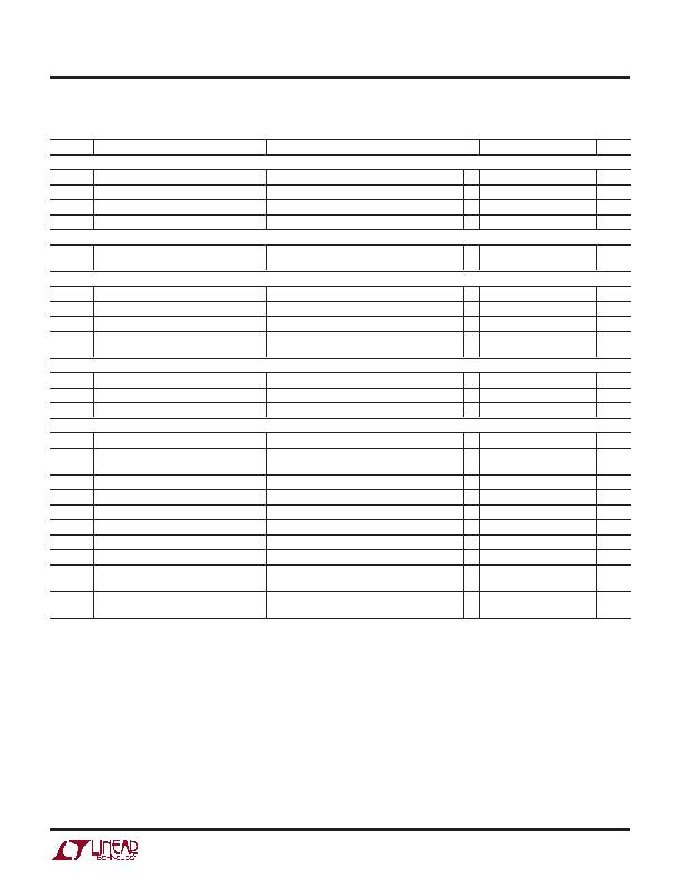
ELECTRICAL CHARACTERISTICS
The q denotes the specifications which apply over the full operating temperature range, otherwise specifications are at T
A
= 25?/SPAN>C.
V
CC
= 2.7V to 5.5V (LTC4302-1), V
CC
= V
CC2
= 2.7V to 5.5V (LTC4302-2) unless otherwise noted.
Note 1: Absolute Maximum Ratings are those values beyond which the life
of a device may be impaired.
Note 2: The I
CC
tests are performed with the backplane-to-card connection
circuitry activated.
Note 3: When the GPIOs are in open-drain output or input mode, the logic
high voltage can be provided by a pull-up supply voltage ranging from
2.2V to 5.5V, independent of the V
CC
voltage.
Note 4: I
PULLUP,AC
varies with temperature and V
CC
voltage as shown in
the Typical Performance Characteristics section.
Note 5: The connection circuitry always regulates its output to a higher
voltage than its input. The magnitude of this offset voltage as a function of
the pull-up resistor and V
CC
voltage is shown in the Typical Performance
Characteristics section.
Note 6: The specifications in this section illustrate the LTC4302-1/
LTC4302-2s compatibility with the I
2
C Fast Mode, the I
2
C Standard Mode
and SMBus specifications. See the Timing Diagram on page 5 for
illustrations of the timing parameters.
Note 7: C
B
= total capacitance of one bus line in pF.
Note 8: The digital interface circuit controls the data fall time only when
acknowledging or transmitting zeros during a read operation. The input-
output connection data and clock outputs meet the fall time specification
provided that the corresponding inputs meet the fall time specification.
Note 9: Guaranteed by design. Not subject to test.
SYMBOL PARAMETER
CONDITIONS
MIN
TYP
MAX
UNITS
General Purpose I/Os
V
LOW
I/O Logic Low Voltage
I
SINK
= 10mA, V
CC
= 2.7V
q
0.36
0.8
V
V
HIGH
I/O Logic High Voltage
I
SOURCE
= 200礎, V
CC
= 2.7V
q
2.4
V
I
LEAK
I/O Leakage Current
V
I/O
= 0V to 5.5V (Note 3)
q
?
礎
V
THRESH
Input Threshold Voltage
Input Mode
q
0.8
1.5
2.2
V
Rise Time Accelerators
I
PULLUP,AC
Transient Boosted Pull-Up Current
Positive Transition on SDA, SCL,
q
1
2
mA
Slew Rate = 0.8V/祍, V
CC
= 2.7V (Note 4)
Input-Output Connection
V
OS
Output-Input Offset Voltage
10k to V
CC
on SDA, SCL Pins (Note 5),
q
0
100
175
mV
C
IN
Digital Input Capacitance
(Note 9)
10
pF
V
OL
Output Low Voltage
SDA, SCL Pins, I
SINK
= 3mA
q
0
0.4
V
I
LEAK
Input Leakage Current
SDA, SCL Pins, V
CC
= 0V to 5.5V
q
?
礎
Connection Circuits Inactive
2-Wire Digital Interface Voltage Characteristics
V
LTH
Logic Threshold Voltage
q 0.3V
CC
0.5V
CC
0.7V
CC
V
I
LEAK
Digital Input Leakage
V
CC
= 0V to 5.5V
q
?
礎
V
OL
Digital Output Low Voltage
I
PULLUP
= 3mA Into SDAIN Pin
q
0.4
V
2-Wire Digital Interface Timing Characteristics (Note 6)
f
I2C,MAX
I
2
C Operating Frequency
(Note 9)
400
600
kHz
t
BUF
Bus Free Time Between Stop and Start
(Note 9)
0.75
1.3
祍
Condition
t
HD,STA
Hold Time After (Repeated) Start Condition (Note 9)
45
100
ns
t
SU,STA
Repeated Start Condition Setup Time
(Note 9)
30
0
ns
t
SU,STO
Stop Condition Setup Time
(Note 9)
30
0
ns
t
HD,DATI
Data Hold Time Input
(Note 9)
25
0
ns
t
HD,DATO
Data Hold Time Output
300
600
900
ns
t
SU,DAT
Data Setup Time
(Note 9)
50
100
ns
t
SP
Pulse Width of Spikes Suppressed by
(Note 9)
50
150
250
ns
the Input Filter
t
f
Data Fall Time
(Notes 7, 8, 9)
20 +
300
ns
0.1C
B
相关PDF资料 |
PDF描述 |
|---|---|
| LTC4303CDD#TRPBF | IC BUS BUFFER I2C 8-DFN |
| LTC4304IDD#TRPBF | IC BUS BUFFER I2C 10-DFN |
| LTC4307IMS8-1#TRPBF | IC BUFFER 2-WIRE BUS 8-MSOP |
| LTC4307IMS8#TRPBF | IC BUS BUFFER I2C 8-MSOP |
| LTC4308IMS8#TRPBF | IC BUS BUFFER LV 8-MSOP |
相关代理商/技术参数 |
参数描述 |
|---|---|
| LTC4302IMS-2 | 功能描述:IC BUFFER BUS 2WR ADDRESS 10MSOP RoHS:否 类别:集成电路 (IC) >> PMIC - 热交换 系列:- 产品培训模块:Obsolescence Mitigation Program 标准包装:100 系列:- 类型:热插拔开关 应用:通用 内部开关:是 电流限制:可调 电源电压:9 V ~ 13.2 V 工作温度:-40°C ~ 150°C 安装类型:表面贴装 封装/外壳:10-WFDFN 裸露焊盘 供应商设备封装:10-TDFN-EP(3x3) 包装:管件 |
| LTC4302IMS-2#PBF | 功能描述:IC BUFFER 2-WIRE BUS 10-MSOP RoHS:是 类别:集成电路 (IC) >> PMIC - 热交换 系列:- 产品培训模块:Obsolescence Mitigation Program 标准包装:100 系列:- 类型:热插拔开关 应用:通用 内部开关:是 电流限制:可调 电源电压:9 V ~ 13.2 V 工作温度:-40°C ~ 150°C 安装类型:表面贴装 封装/外壳:10-WFDFN 裸露焊盘 供应商设备封装:10-TDFN-EP(3x3) 包装:管件 |
| LTC4302IMS-2#TR | 功能描述:IC BUFFER BUS 2WR ADDRESS 10MSOP RoHS:否 类别:集成电路 (IC) >> PMIC - 热交换 系列:- 产品培训模块:Obsolescence Mitigation Program 标准包装:100 系列:- 类型:热插拔开关 应用:通用 内部开关:是 电流限制:可调 电源电压:9 V ~ 13.2 V 工作温度:-40°C ~ 150°C 安装类型:表面贴装 封装/外壳:10-WFDFN 裸露焊盘 供应商设备封装:10-TDFN-EP(3x3) 包装:管件 |
| LTC4302IMS-2#TRPBF | 功能描述:IC BUFFER 2-WIRE BUS 10-MSOP RoHS:是 类别:集成电路 (IC) >> PMIC - 热交换 系列:- 产品培训模块:Obsolescence Mitigation Program 标准包装:100 系列:- 类型:热插拔开关 应用:通用 内部开关:是 电流限制:可调 电源电压:9 V ~ 13.2 V 工作温度:-40°C ~ 150°C 安装类型:表面贴装 封装/外壳:10-WFDFN 裸露焊盘 供应商设备封装:10-TDFN-EP(3x3) 包装:管件 |
| LTC4303CDD | 制造商:Linear Technology 功能描述:Hot Swappable Bus Buffer 8-Pin DFN EP |
发布紧急采购,3分钟左右您将得到回复。