- 您现在的位置:买卖IC网 > PDF目录67759 > LTC4355IMS#PBF (LINEAR TECHNOLOGY CORP) 2-CHANNEL POWER SUPPLY SUPPORT CKT, PDSO16 PDF资料下载
参数资料
| 型号: | LTC4355IMS#PBF |
| 厂商: | LINEAR TECHNOLOGY CORP |
| 元件分类: | 电源管理 |
| 英文描述: | 2-CHANNEL POWER SUPPLY SUPPORT CKT, PDSO16 |
| 封装: | LEAD FREE, PLASTIC, MSOP-16 |
| 文件页数: | 20/20页 |
| 文件大小: | 249K |
| 代理商: | LTC4355IMS#PBF |
LTC4355
9
4355fe
APPLICATIONS INFORMATION
System Power Supply Failure
The LTC4355 automatically supplies load current from the
system input supply with the higher voltage. If this supply
shorts to ground, reverse current begins to ow through
the pass transistor temporarily and the transistor begins
to turn off. When this reverse current creates –25mV of
voltage drop across the drain and source pins of the pass
transistor, a fast pull-down circuit engages to drive the
gate low faster.
The remaining system power supply delivers the load cur-
rent through the body diode of its pass transistor until the
channel turns on. The LTC4355 ramps the gate up with
20μA, turning on the N-channel MOSFET to reduce the
voltage drop across it.
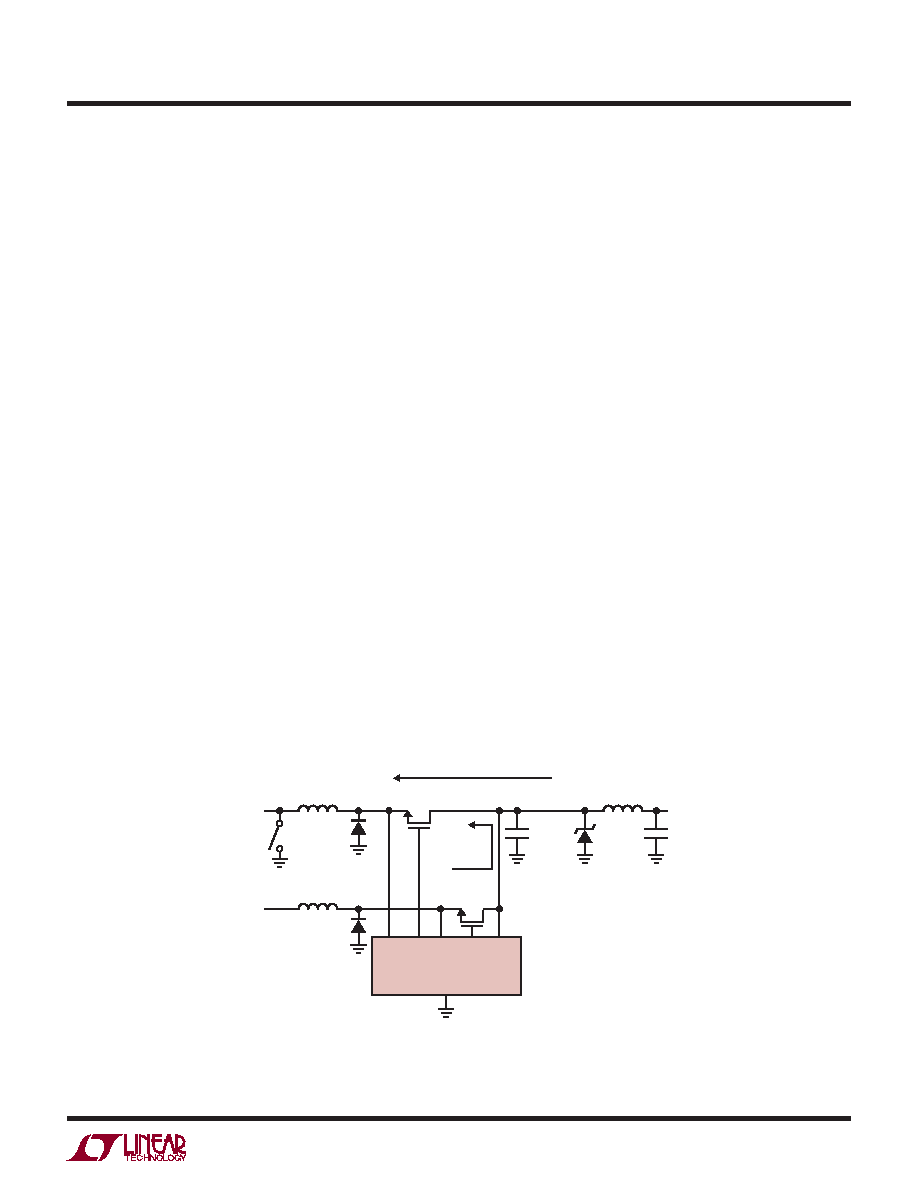
Input Short-Circuit Faults
The dynamic behavior of an active, ideal diode entering
reverse bias is most accurately characterized by a delay
followed by a period of reverse recovery. During the delay
phase some reverse current is built up, limited by para-
sitic resistances and inductances. During the reverse re-
covery phase, energy stored in the parasitic inductances
is transferred to other elements in the circuit. Current
slew rates during reverse recovery may reach 100A/μs
or higher.
High slew rates coupled with parasitic inductances in se-
ries with the input and output paths may cause potentially
destructive transients to appear at the IN and OUT pins of
the LTC4355 during reverse recovery. A zero impedance
short-circuit directly across an input that is supplying
current is especially troublesome because it permits the
highest possible reverse current to build up during the
delay phase. When the MOSFET nally commutates the
reverse current the LTC4355 IN pin experiences a nega-
tive voltage spike, while the OUT pin spikes in the positive
direction.
To prevent damage to the LTC4355 under conditions of
input short-circuit, protect the IN pins and OUT pin as
shown in Figure 1. The IN pins are protected by clamping
to the GND pin in the negative direction. Protect the OUT
pin with a clamp, such as with a TVS or TransZorb, or with
a local bypass capacitor of at least 10μF. In low voltage
applications the MOSFET’s drain-source breakdown may
be sufcient to protect the OUT pin, provided BVDSS +
VIN < 100V.
Parasitic inductance between the load bypass or the
second supply and the LTC4355 allows a zero impedance
input short to collapse the voltage at the OUT pin, which
increases the total turn-off time (tOFF). For applications
up to 30V, bypass the OUT pin with 39μF; above 30V use
at least 100μF. One capacitor serves to guard against OUT
collapse and also protect OUT from voltage spikes.
Figure 1. Reverse Recovery Produces Inductive Spikes at the IN and OUT Pins.
The Polarity of Step Recovery Spikes Is Shown Across Parasitic Inductances
LTC4355
GND
GATE1
GATE2
IN1
OUT
IN2
M1
FDS3672
REVERSE
RECOVERY
CURRENT
M2
FDS3672
VIN1
VOUT
VIN2
DIN2
SBR1U150SA
INPUT PARASITIC
INDUCTANCE
+
–
OUTPUT PARASITIC
INDUCTANCE
+
–
INPUT PARASITIC
INDUCTANCE
–
+
COUT
10μF
CLOAD
DCLAMP
SMAT70A
OR
REVERSE RECOVERY CURRENT
4355 F01
DIN1
SBR1U150SA
INPUT
SHORT
相关PDF资料 |
PDF描述 |
|---|---|
| LTC4416EMS#TR | 1-CHANNEL POWER SUPPLY SUPPORT CKT, PDSO10 |
| LTC4416EMS-1#TR | 1-CHANNEL POWER SUPPLY SUPPORT CKT, PDSO10 |
| LTC4416IMS-1#TR | 1-CHANNEL POWER SUPPLY SUPPORT CKT, PDSO10 |
| LTC4416IMS#TR | 1-CHANNEL POWER SUPPLY SUPPORT CKT, PDSO10 |
| LTC6405CMS8E#TRPBF | SPECIALTY ANALOG CIRCUIT, PDSO8 |
相关代理商/技术参数 |
参数描述 |
|---|---|
| LTC4355IS#PBF | 功能描述:IC IDEAL DIODE-OR 16-SOIC RoHS:是 类别:集成电路 (IC) >> PMIC - O 圈控制器 系列:- 标准包装:1,000 系列:- 应用:电池备份,工业/汽车,大电流开关 FET 型:- 输出数:5 内部开关:是 延迟时间 - 开启:100ns 延迟时间 - 关闭:- 电源电压:3 V ~ 5.5 V 电流 - 电源:250µA 工作温度:0°C ~ 70°C 安装类型:表面贴装 封装/外壳:16-SOIC(0.154",3.90mm 宽) 供应商设备封装:16-SOIC N 包装:带卷 (TR) |
| LTC4355IS#PBF | 制造商:Linear Technology 功能描述:Power Management IC |
| LTC4355IS#TRPBF | 功能描述:IC IDEAL DIODE-OR 16-SOIC RoHS:是 类别:集成电路 (IC) >> PMIC - O 圈控制器 系列:- 标准包装:1,000 系列:- 应用:电池备份,工业/汽车,大电流开关 FET 型:- 输出数:5 内部开关:是 延迟时间 - 开启:100ns 延迟时间 - 关闭:- 电源电压:3 V ~ 5.5 V 电流 - 电源:250µA 工作温度:0°C ~ 70°C 安装类型:表面贴装 封装/外壳:16-SOIC(0.154",3.90mm 宽) 供应商设备封装:16-SOIC N 包装:带卷 (TR) |
| LTC4355ISPBF | 制造商:Linear Technology 功能描述:Ideal Diode-OR Controller 9-80V SOIC16 |
| LTC4357CDCB#PBF | 制造商:Linear Technology 功能描述:CONTROLLER DIODE SMD DFN-6 4357 制造商:Linear Technology 功能描述:IDEAL DIODE CONTROLLER, 80V, DFN-6; IC Function:Ideal Diode Controller; Supply Voltage Min:9V; Supply Voltage Max:80V; Operating Temperature Min:0C; Operating Temperature Max:70C; Digital IC Case Style:DFN; No. of Pins:6 ;RoHS Compliant: Yes |
发布紧急采购,3分钟左右您将得到回复。