- 您现在的位置:买卖IC网 > PDF目录44997 > LTC4357MPMS8#TR (LINEAR TECHNOLOGY CORP) 1-CHANNEL POWER SUPPLY SUPPORT CKT, PDSO8 PDF资料下载
参数资料
| 型号: | LTC4357MPMS8#TR |
| 厂商: | LINEAR TECHNOLOGY CORP |
| 元件分类: | 电源管理 |
| 英文描述: | 1-CHANNEL POWER SUPPLY SUPPORT CKT, PDSO8 |
| 封装: | PLASTIC, MSOP-8 |
| 文件页数: | 12/14页 |
| 文件大小: | 723K |
| 代理商: | LTC4357MPMS8#TR |
LTC4357
4357fd
applications inForMation
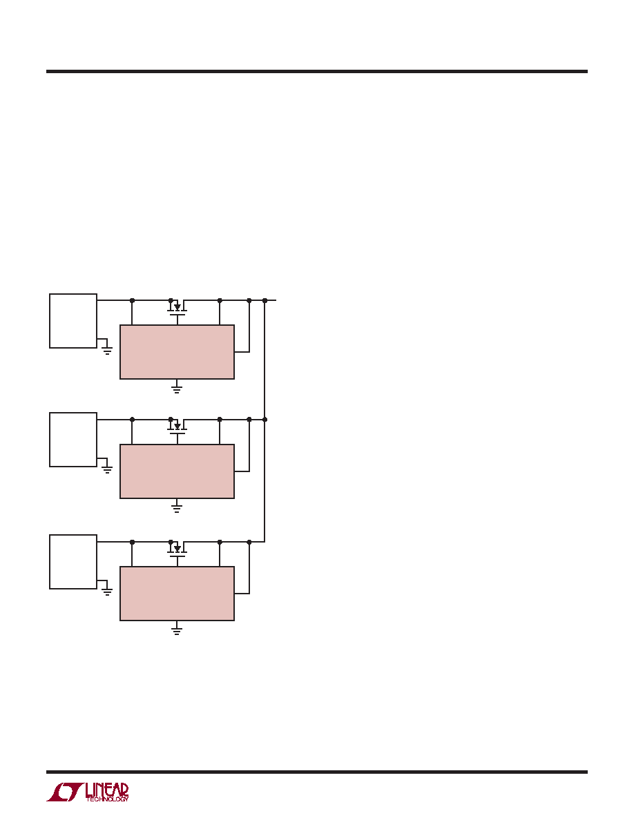
Figure 1. Droop Sharing Redundant Supplies
4357 F01
LTC4357
GND
IN
OUT
VDD
GATE
M1
FDB3632
48V BUS
LTC4357
GND
IN
OUT
VDD
GATE
M2
FDB3632
LTC4357
GND
IN
OUT
VDD
PSA
VINA
48V
RTNA
GATE
M3
FDB3632
PSB
VINB
48V
RTNB
PSC
VINC
48V
RTNC
Load Sharing
TheapplicationinFigure1combinestheoutputsofmultiple,
redundant supplies using a simple technique known as
droop sharing. Load current is first taken from the highest
output, with the low outputs contributing as the output
voltagefallsunderincreasedloading.The25mVregulation
technique ensures smooth load sharing between outputs
without oscillation. The degree of sharing is a function of
RDS(ON), the output impedance of the supplies and their
initial output voltages.
Input Short-Circuit Faults
The dynamic behavior of an active, ideal diode entering
reverse bias is most accurately characterized by a delay
followed by a period of reverse recovery. During the delay
phase some reverse current is built up, limited by parasitic
resistances and inductances. During the reverse recovery
phase, energy stored in the parasitic inductances is trans-
ferred to other elements in the circuit. Current slew rates
during reverse recovery may reach 100A/s or higher.
High slew rates coupled with parasitic inductances in se-
ries with the input and output paths may cause potentially
destructive transients to appear at the IN and OUT pins
of the LTC4357 during reverse recovery. A zero imped-
ance short-circuit directly across the input of the circuit
is especially troublesome because it permits the highest
possiblereversecurrenttobuildupduringthedelayphase.
When the MOSFET finally commutates the reverse current
the LTC4357 IN pin experiences a negative voltage spike,
while the OUT pin spikes in the positive direction.
To prevent damage to the LTC4357 under conditions of
input short-circuit, protect the IN pin and OUT pin as
shown in Figure 2. The IN pin is protected by clamping
to the GND pin in the negative direction. Protect the OUT
pin with a clamp, such as with a TVS or TransZorb, or with
a local bypass capacitor of at least 10F. In low voltage
applications the MOSFET's drain-source breakdown may
be sufficient to protect the OUT pin, provided BVDSS +
VIN < 100V.
Parasitic inductance between the load bypass and the
LTC4357 allows a zero impedance input short to collapse
thevoltageattheVDDpin,whichincreasesthetotalturn-off
time (tOFF). For applications up to 30V, bypass the VDD pin
with 39F; above 30V use at least 100F. If VDD is powered
fromtheoutputside,onecapacitorservestoguardagainst
VDD collapse and also protect OUT from voltage spikes.
If the OUT pin is protected by a diode clamp or if VDD is
powered from the input side, decouple the VDD pin with a
separate 100, 100nF filter (see Figure 3). In applications
above 10A increase the filter capacitor to 1F.
相关PDF资料 |
PDF描述 |
|---|---|
| LTC4360CSC8-2#TRPBF | 1-CHANNEL POWER SUPPLY SUPPORT CKT, PDSO8 |
| LTC4360ISC8-1#TRMPBF | 1-CHANNEL POWER SUPPLY SUPPORT CKT, PDSO8 |
| LTC4365CTS8#TRMPBF | 1-CHANNEL POWER SUPPLY SUPPORT CKT, PDSO8 |
| LTC4365HDDB#TRMPBF | 1-CHANNEL POWER SUPPLY SUPPORT CKT, PDSO8 |
| LTC4365HDDB#TRPBF | 1-CHANNEL POWER SUPPLY SUPPORT CKT, PDSO8 |
相关代理商/技术参数 |
参数描述 |
|---|---|
| LTC4358CDE#PBF | 功能描述:IC IDEAL DIODE 5A 14-DFN RoHS:是 类别:集成电路 (IC) >> PMIC - O 圈控制器 系列:- 标准包装:1,000 系列:- 应用:电池备份,工业/汽车,大电流开关 FET 型:- 输出数:5 内部开关:是 延迟时间 - 开启:100ns 延迟时间 - 关闭:- 电源电压:3 V ~ 5.5 V 电流 - 电源:250µA 工作温度:0°C ~ 70°C 安装类型:表面贴装 封装/外壳:16-SOIC(0.154",3.90mm 宽) 供应商设备封装:16-SOIC N 包装:带卷 (TR) |
| LTC4358CDE#TRPBF | 功能描述:IC IDEAL DIODE 5A 14-DFN RoHS:是 类别:集成电路 (IC) >> PMIC - O 圈控制器 系列:- 标准包装:1,000 系列:- 应用:电池备份,工业/汽车,大电流开关 FET 型:- 输出数:5 内部开关:是 延迟时间 - 开启:100ns 延迟时间 - 关闭:- 电源电压:3 V ~ 5.5 V 电流 - 电源:250µA 工作温度:0°C ~ 70°C 安装类型:表面贴装 封装/外壳:16-SOIC(0.154",3.90mm 宽) 供应商设备封装:16-SOIC N 包装:带卷 (TR) |
| LTC4358CFE#PBF | 功能描述:IC IDEAL DIODE 5A 16-TSSOP RoHS:是 类别:集成电路 (IC) >> PMIC - O 圈控制器 系列:- 标准包装:1,000 系列:- 应用:电池备份,工业/汽车,大电流开关 FET 型:- 输出数:5 内部开关:是 延迟时间 - 开启:100ns 延迟时间 - 关闭:- 电源电压:3 V ~ 5.5 V 电流 - 电源:250µA 工作温度:0°C ~ 70°C 安装类型:表面贴装 封装/外壳:16-SOIC(0.154",3.90mm 宽) 供应商设备封装:16-SOIC N 包装:带卷 (TR) |
| LTC4358CFE#TRPBF | 功能描述:IC IDEAL DIODE 5A 16-TSSOP RoHS:是 类别:集成电路 (IC) >> PMIC - O 圈控制器 系列:- 标准包装:1,000 系列:- 应用:电池备份,工业/汽车,大电流开关 FET 型:- 输出数:5 内部开关:是 延迟时间 - 开启:100ns 延迟时间 - 关闭:- 电源电压:3 V ~ 5.5 V 电流 - 电源:250µA 工作温度:0°C ~ 70°C 安装类型:表面贴装 封装/外壳:16-SOIC(0.154",3.90mm 宽) 供应商设备封装:16-SOIC N 包装:带卷 (TR) |
| LTC4358IDE#PBF | 功能描述:IC IDEAL DIODE 5A 14-DFN RoHS:是 类别:集成电路 (IC) >> PMIC - O 圈控制器 系列:- 标准包装:1,000 系列:- 应用:电池备份,工业/汽车,大电流开关 FET 型:- 输出数:5 内部开关:是 延迟时间 - 开启:100ns 延迟时间 - 关闭:- 电源电压:3 V ~ 5.5 V 电流 - 电源:250µA 工作温度:0°C ~ 70°C 安装类型:表面贴装 封装/外壳:16-SOIC(0.154",3.90mm 宽) 供应商设备封装:16-SOIC N 包装:带卷 (TR) |
发布紧急采购,3分钟左右您将得到回复。