- 您现在的位置:买卖IC网 > PDF目录10203 > LTC485CN8 (Linear Technology)IC TXRX INTRFC RS485 LOPWR 8-DIP PDF资料下载
参数资料
| 型号: | LTC485CN8 |
| 厂商: | Linear Technology |
| 文件页数: | 13/14页 |
| 文件大小: | 0K |
| 描述: | IC TXRX INTRFC RS485 LOPWR 8-DIP |
| 标准包装: | 50 |
| 类型: | 收发器 |
| 驱动器/接收器数: | 1/1 |
| 规程: | RS485 |
| 电源电压: | 4.75 V ~ 5.25 V |
| 安装类型: | 通孔 |
| 封装/外壳: | 8-DIP(0.300",7.62mm) |
| 供应商设备封装: | 8-PDIP |
| 包装: | 管件 |
LTC485
8
485fk
For more information www.linear.com/LTC485
Basic Theory of Operation
Previous RS485 transceivers have been designed using
bipolar technology because the common mode range
of the device must extend beyond the supplies and the
device must be immune to ESD damage and latchup.
Unfortunately, the bipolar devices draw a large amount of
supply current, which is unacceptable for the numerous
applications that require low power consumption. The
LTC485 is the first CMOS RS485/RS422 transceiver which
features ultralow power consumption without sacrificing
ESD and latchup immunity.
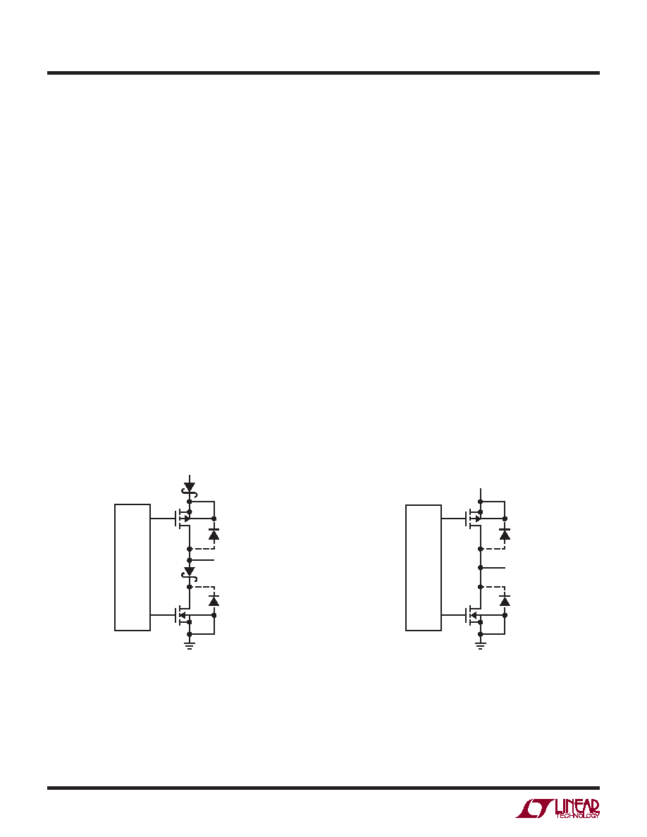
The LTC485 uses a proprietary driver output stage, which
allows a common-mode range that extends beyond the
power supplies while virtually eliminating latchup and
providing excellent ESD protection. Figure 9 shows the
LTC485outputstagewhileFigure10showsaconventional
CMOS output stage.
When the conventional CMOS output stage of Figure 10
enters a high impedance state, both the P-channel (P1)
and the N-channel (N1) are turned off. If the output is
then driven above VCC or below ground, the P + /N-well
Figure 9. LTC485 Output Stage
diode (D1) or the N + /P-substrate diode (D2) respectively
will turn on and clamp the output to the supply. Thus,
the output stage is no longer in a high impedance state
and is not able to meet the RS485 common mode range
requirement. In addition, the large amount of current
flowing through either diode will induce the well known
CMOS latchup condition, which could destroy the device.
The LTC485 output stage of Figure 9 eliminates these
problems by adding two Schottky diodes, SD3 and SD4.
The Schottky diodes are fabricated by a proprietary modi-
fication to the standard N-well CMOS process. When the
output stage is operating normally, the Schottky diodes
are forward biased and have a small voltage drop across
them. When the output is in the high impedance state and
is driven above VCC or below ground, the parasitic diodes
D1 or D2 still turn on, but SD3 or SD4 will reverse bias
and prevent current from flowing into the N-well or the
substrate. Thus, the high impedance state is maintained
even with the output voltage beyond the supplies. With
no minority carrier current flowing into the N-well or
substrate, latchup is virtually eliminated under power-up
or power-down conditions.
APPLICATIONS INFORMATION
Figure 10. Conventional CMOS Output Stage
LOGIC
VCC
SD3
P1
D1
OUTPUT
SD4
D2
N1
485 F09
LOGIC
VCC
P1
D1
OUTPUT
D2
N1
485 F10
相关PDF资料 |
PDF描述 |
|---|---|
| 13280-20SG-326 | CONN PLUG 20POS CABLE SKT |
| MS27472T20F35P | CONN RCPT 79POS WALL MNT W/PINS |
| LTC2246CUH#TRPBF | IC ADC 14BIT 25MSPS SAMPL 32-QFN |
| SP3226ECA-L | IC TXRX RS232 ESD SD 16SSOP |
| MS27472E14A18PA | CONN RCPT 18POS WALL MT W/PINS |
相关代理商/技术参数 |
参数描述 |
|---|---|
| LTC485CN8#PBF | 功能描述:IC TXRX INTRFC RS485 LOPWR 8-DIP RoHS:是 类别:集成电路 (IC) >> 接口 - 驱动器,接收器,收发器 系列:- 标准包装:98 系列:* |
| LTC485CN8PBF | 制造商:Linear Technology 功能描述:LTC485CN8PBF |
| LTC485CS8 | 功能描述:IC TXRX INTRFC RS485 LOPWR 8SOIC RoHS:否 类别:集成电路 (IC) >> 接口 - 驱动器,接收器,收发器 系列:- 标准包装:121 系列:- 类型:收发器 驱动器/接收器数:1/1 规程:RS422,RS485 电源电压:3 V ~ 3.6 V 安装类型:表面贴装 封装/外壳:10-WFDFN 裸露焊盘 供应商设备封装:10-DFN(3x3) 包装:管件 |
| LTC485CS8#PBF | 功能描述:IC TXRX INTRFC RS485 LOPWR 8SOIC RoHS:是 类别:集成电路 (IC) >> 接口 - 驱动器,接收器,收发器 系列:- 产品培训模块:RS-232 & USB Transceiver 标准包装:2,000 系列:- 类型:收发器 驱动器/接收器数:1/1 规程:RS232 电源电压:3 V ~ 5.5 V 安装类型:表面贴装 封装/外壳:16-SSOP(0.209",5.30mm 宽) 供应商设备封装:16-SSOP 包装:带卷 (TR) 其它名称:296-19849-2 |
| LTC485CS8#TR | 功能描述:IC TXRX INTRFC RS485 LOPWR 8SOIC RoHS:否 类别:集成电路 (IC) >> 接口 - 驱动器,接收器,收发器 系列:- 标准包装:121 系列:- 类型:收发器 驱动器/接收器数:1/1 规程:RS422,RS485 电源电压:3 V ~ 3.6 V 安装类型:表面贴装 封装/外壳:10-WFDFN 裸露焊盘 供应商设备封装:10-DFN(3x3) 包装:管件 |
发布紧急采购,3分钟左右您将得到回复。