- 您现在的位置:买卖IC网 > PDF目录3514 > LTC6079CGN#TRPBF (Linear Technology)IC OP AMP QUAD R-R I/O 16SSOP PDF资料下载
参数资料
| 型号: | LTC6079CGN#TRPBF |
| 厂商: | Linear Technology |
| 文件页数: | 20/20页 |
| 文件大小: | 0K |
| 描述: | IC OP AMP QUAD R-R I/O 16SSOP |
| 标准包装: | 2,500 |
| 放大器类型: | 通用 |
| 电路数: | 4 |
| 输出类型: | 满摆幅 |
| 转换速率: | 0.05 V/µs |
| 增益带宽积: | 750kHz |
| 电流 - 输入偏压: | 0.2pA |
| 电压 - 输入偏移: | 10µV |
| 电流 - 电源: | 55µA |
| 电流 - 输出 / 通道: | 25mA |
| 电压 - 电源,单路/双路(±): | 2.7 V ~ 5.5 V |
| 工作温度: | 0°C ~ 70°C |
| 安装类型: | 表面贴装 |
| 封装/外壳: | 16-SSOP(0.154",3.90mm 宽) |
| 供应商设备封装: | 16-SSOP |
| 包装: | 带卷 (TR) |
LTC6078/LTC6079
9
60789fa
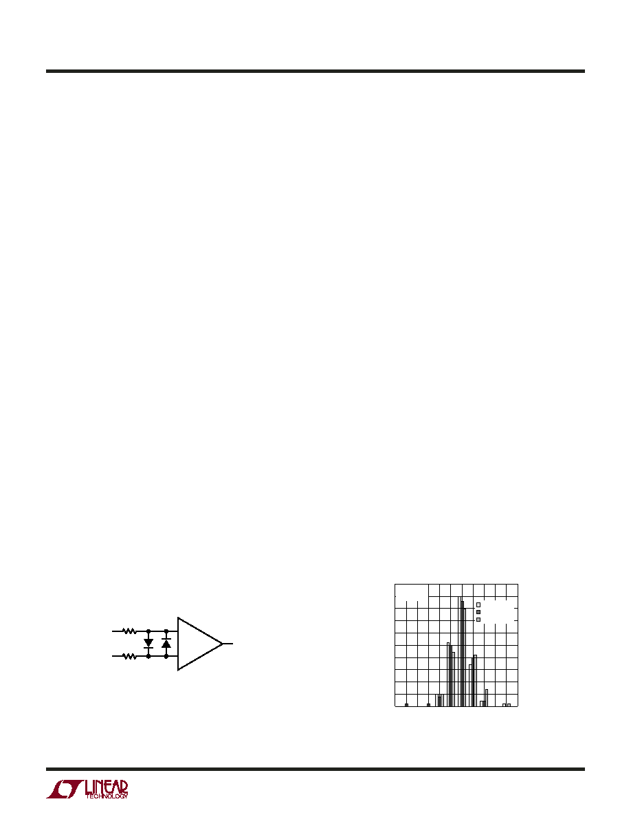
Figure 1. Op Amp with Input Voltage Clamp
Preserving Input Precision
Preserving input accuracy of the LTC6078/LTC6079 re-
quires that the application circuit and PC board layout do
not introduce errors comparable or greater than the 10V
typical offset of the ampliers. Temperature differentials
across the input connections can generate thermocouple
voltages of 10’s of microvolts so the connections to the
input leads should be short, close together and away from
heat dissipating components. Air current across the board
can also generate temperature differentials.
The extremely low input bias currents (0.2pA typical) al-
low high accuracy to be maintained with high impedance
sources and feedback resistors. Leakage currents on the
PC board can be higher than the input bias current. For
example, 10GΩ of leakage between a 5V supply lead and
an input lead will generate 500pA! Surround the input
leads with a guard ring driven to the same potential as the
input common mode to avoid excessive leakage in high
impedance applications.
Input Clamps
Large differential voltages across the inputs over very
long time periods can impact the precisely trimmed input
offset voltage of the LTC6078/LTC6079. As an example,
a 2V differential voltage between the inputs over a period
of 100 hours can shift the input offset voltage by tens
of microvolts. If the amplier is to be subjected to large
differential input voltages, adding back-to-back diodes
between the two inputs will minimize this shift and retain
the DC precision. If necessary, current-limiting series
resistors can be added in front of the diodes, as shown
in Figure 1. These diodes are not necessary for normal
closed loop applications.
–
+
500
500
60789 F01
APPLICATIO S I FOR ATIO
WU
U
Capacitive Load
LTC6078/LTC6079 can drive capactive load up to 200pF in
unity gain. The capacitive load driving capability increases
as the amplier is used in higher gain congurations. A
small series resistance between the ouput and the load
further increases the amount of capacitance the amplier
can drive.
SHDN Pins
Pins 5 and 6 are used for power shutdown on the LTC6078
in the DD package. If they are oating, internal current
sources pull Pins 5 and 6 to V+ and the ampliers operate
normally. In shutdown, the amplier output is high imped-
ance, and each amplier draws less than 2A current.
When the chip is turned on, the supply current per amplier
is about 35A larger than its normal values for 50s.
Rail-to-Rail Input
The input stage of LTC6078/LTC6079 combines both PMOS
and NMOS differential pairs, extending its input common
mode voltage range to both positive and negative supply
voltages. At high input common mode range, the NMOS
pair is on. At low common mode range, the PMOS pair is
on. The transition happens when the common voltage is
between 1.3V and 0.9V below the positive supply.
Thermal Hysteresis
Figure 2 shows the input offset hysteresis of LTC6078MS8
for 3 thermal cycles from –45°C to 90°C. The typical offset
shift after the 3 cycles is only 1V.
Figure 2. VOS Thermal Hysteresis of LTC6078MS8
VOS CHANGE FROM INITIAL VALUE
NUMBER
OF
AMPLIFIERS
50
45
40
35
30
25
20
15
10
5
0
60789 F02
–5
5
–3
–4
–2 –1
2
4
6
01
3
VS = 3V
VCM = 0.5V
1ST CYCLE
2ND CYCLE
3RD CYCLE
相关PDF资料 |
PDF描述 |
|---|---|
| LTC2050HVHS6#TRMPBF | IC OP AMP ZERO-DRIFT SOT23-6 |
| LTC6079CGN#TR | IC OP AMP QUAD R-R I/O 16SSOP |
| MAX4163ESA+ | IC OPAMP MICROPWR DUAL R-R 8SOIC |
| RMCF0805FT150R | RES 150 OHM 1/8W 1% 0805 SMD |
| LTC2050HVHS6#TRM | IC OP AMP ZERO-DRIFT SOT23-6 |
相关代理商/技术参数 |
参数描述 |
|---|---|
| LTC6079HGN | 功能描述:IC OP AMP QUAD R-R I/O 16SSOP RoHS:否 类别:集成电路 (IC) >> Linear - Amplifiers - Instrumentation 系列:- 标准包装:100 系列:- 放大器类型:通用 电路数:1 输出类型:- 转换速率:0.2 V/µs 增益带宽积:- -3db带宽:- 电流 - 输入偏压:100pA 电压 - 输入偏移:30µV 电流 - 电源:380µA 电流 - 输出 / 通道:- 电压 - 电源,单路/双路(±):±2 V ~ 18 V 工作温度:0°C ~ 70°C 安装类型:表面贴装 封装/外壳:8-SOIC(0.154",3.90mm 宽) 供应商设备封装:8-SO 包装:管件 |
| LTC6079HGN#PBF | 功能描述:IC OP AMP QUAD R-R I/O 16SSOP RoHS:是 类别:集成电路 (IC) >> Linear - Amplifiers - Instrumentation 系列:- 标准包装:100 系列:- 放大器类型:通用 电路数:1 输出类型:- 转换速率:0.2 V/µs 增益带宽积:- -3db带宽:- 电流 - 输入偏压:100pA 电压 - 输入偏移:30µV 电流 - 电源:380µA 电流 - 输出 / 通道:- 电压 - 电源,单路/双路(±):±2 V ~ 18 V 工作温度:0°C ~ 70°C 安装类型:表面贴装 封装/外壳:8-SOIC(0.154",3.90mm 宽) 供应商设备封装:8-SO 包装:管件 |
| LTC6079HGN#TR | 功能描述:IC OP AMP QUAD R-R I/O 16SSOP RoHS:否 类别:集成电路 (IC) >> Linear - Amplifiers - Instrumentation 系列:- 标准包装:50 系列:- 放大器类型:J-FET 电路数:2 输出类型:- 转换速率:3.5 V/µs 增益带宽积:1MHz -3db带宽:- 电流 - 输入偏压:30pA 电压 - 输入偏移:2000µV 电流 - 电源:200µA 电流 - 输出 / 通道:- 电压 - 电源,单路/双路(±):7 V ~ 36 V,±3.5 V ~ 18 V 工作温度:0°C ~ 70°C 安装类型:通孔 封装/外壳:8-DIP(0.300",7.62mm) 供应商设备封装:8-PDIP 包装:管件 |
| LTC6079HGN#TRPBF | 功能描述:IC OP AMP QUAD R-R I/O 16SSOP RoHS:是 类别:集成电路 (IC) >> Linear - Amplifiers - Instrumentation 系列:- 标准包装:50 系列:- 放大器类型:J-FET 电路数:2 输出类型:- 转换速率:3.5 V/µs 增益带宽积:1MHz -3db带宽:- 电流 - 输入偏压:30pA 电压 - 输入偏移:2000µV 电流 - 电源:200µA 电流 - 输出 / 通道:- 电压 - 电源,单路/双路(±):7 V ~ 36 V,±3.5 V ~ 18 V 工作温度:0°C ~ 70°C 安装类型:通孔 封装/外壳:8-DIP(0.300",7.62mm) 供应商设备封装:8-PDIP 包装:管件 |
| LTC6079IDHC | 功能描述:IC OP AMP QUAD R-R I/O 16DFN RoHS:否 类别:集成电路 (IC) >> Linear - Amplifiers - Instrumentation 系列:- 标准包装:100 系列:- 放大器类型:通用 电路数:1 输出类型:- 转换速率:0.2 V/µs 增益带宽积:- -3db带宽:- 电流 - 输入偏压:100pA 电压 - 输入偏移:30µV 电流 - 电源:380µA 电流 - 输出 / 通道:- 电压 - 电源,单路/双路(±):±2 V ~ 18 V 工作温度:0°C ~ 70°C 安装类型:表面贴装 封装/外壳:8-SOIC(0.154",3.90mm 宽) 供应商设备封装:8-SO 包装:管件 |
发布紧急采购,3分钟左右您将得到回复。