参数资料
| 型号: | LTC6085HDHC#TRPBF |
| 厂商: | Linear Technology |
| 文件页数: | 2/16页 |
| 文件大小: | 0K |
| 描述: | IC AMP R-R CMOS QUAD 16-DFN |
| 标准包装: | 2,500 |
| 放大器类型: | 通用 |
| 电路数: | 4 |
| 输出类型: | 满摆幅 |
| 转换速率: | 0.5 V/µs |
| 增益带宽积: | 1.5MHz |
| 电流 - 输入偏压: | 1pA |
| 电压 - 输入偏移: | 300µV |
| 电流 - 电源: | 110µA |
| 电流 - 输出 / 通道: | 12.5mA |
| 电压 - 电源,单路/双路(±): | 2.5 V ~ 5.5 V |
| 工作温度: | -40°C ~ 125°C |
| 安装类型: | 表面贴装 |
| 封装/外壳: | 16-WFDFN 裸露焊盘 |
| 供应商设备封装: | 16-DFN-EP(5x3) |
| 包装: | 带卷 (TR) |
LTC6084/LTC6085
10
60845fa
APPLICATIONS INFORMATION
Rail-to-Rail Input
The input stage of LTC6084/LTC6085 combines both PMOS
and NMOS differential pairs, extending its input common
mode voltage to both positive and negative supply volt-
ages. At high input common mode range, NMOS pair is
on. At low common mode range, the PMOS pair is on. The
transition happens when the common voltage is between
1.3 and 0.9V below the positive supply.
Achieving Low Input Bias Current
The DD and DHC packages are leadless and make contact
to the PCB beneath the package. Solder ux used during
the attachment of the part to the PCB can create leakage
current paths and can degrade the input bias current per-
formance of the part. All inputs are susceptible because
the backside paddle is connected to V– internally. As the
input voltage or V– changes, a leakage path can be formed
and alter the observed input bias current. For lowest bias
current use the LTC6084/LTC6085 in the leaded MSOP/GN
package. With ne PCB design rules, you can also provide
a guard ring around the inputs.
For example, in high source impedance applications such as
pH probes, photo diodes, strain gauges, etc., the low input
bias current of these parts requires a clean board layout to
minimize additional leakage current into a high impedance
signal node. A mere 100GΩ of PC board resistance between
a 5V supply trace and input trace near ground potential
adds 50pA of leakage current. This leakage is far greater
than the bias current of the operational amplier. A guard
ring around the high impedance input traces driven by a
low impedance source equal to the input voltage prevents
such leakage problems. The guard ring should extend
as far as necessary to shield the high impedance signal
from any and all leakage paths. Figure 1 shows the use
of a guard ring in a unity-gain conguration. In this case
the guard ring is connected to the output and is shielding
the high impedance noninverting input from V–. Figure 2
shows the inverting gain conguration.
Rail-to-Rail Output
The output stage of the LTC6084/LTC6085 swings within
5mV of the supply rails when driving high impedance
loads, in other words when no DC load current is present.
See the Typical Performance Characteristics for curves of
output swing versus load current. The class AB design of
the output stage enables the op amp to supply load cur-
rents which are much greater than the quiescent supply
current. For example, the room temperature short-circuit
current is typically 12.5mA.
Capacitive Load
LTC6084/LTC6085 can drive a capacitive load up to 300pF in
unity gain. The capacitive load driving capability increases
as the amplier is used in higher gain congurations. A
small series resistance between the output and the load
further increases the amount of capacitance the amplier
can drive.
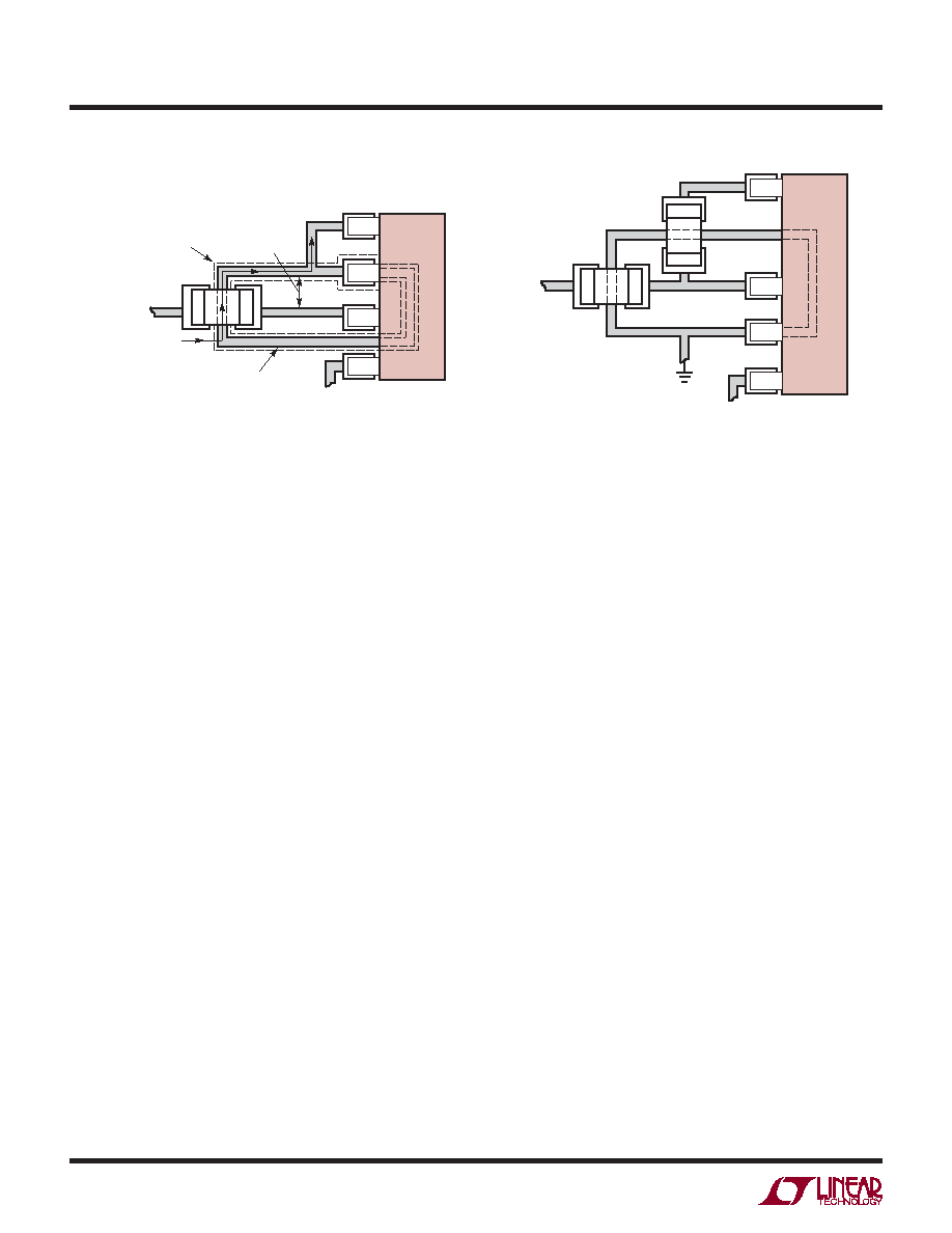
Figure 1. Sample Layout. Unity-Gain Conguration. Using Guard
Ring to Shield High Impedance Input from Board Leakage
Figure 2. Sample Layout. Inverting Gain Conguration. Using
Guard Ring to Shield High Impedance Input from Board Leakage
LTC6084
R
OUT
IN–
IN+
V–
LEAKAGE
CURRENT
NO LEAKAGE
CURRENT
GUARD
RING
NO SOLDER MASK
OVER THE GUARD RING
60845 F01
LTC6084
60845 F02
R
OUT
IN–
IN+
V–
VIN
GND
相关PDF资料 |
PDF描述 |
|---|---|
| LTC6088HGN#TRPBF | IC AMP QUAD CMOS R-R 16-SSOP |
| LTC6101HVAHS5#TRPBF | IC AMP CURRENT SENSE TSOT23-5 |
| LTC6102HMS8-1#TRPBF | IC AMP CURRENT SENSE 8-MSOP |
| LTC6103HMS8#TRPBF | IC AMP CURRENT SENSE 8-MSOP |
| LTC6104CMS8#PBF | IC AMP CURRENT SENSE 8-MSOP |
相关代理商/技术参数 |
参数描述 |
|---|---|
| LTC6085HGN#PBF | 制造商:Linear Technology 功能描述:IC OPAMP GP 1.5MHZ RRO 16SSOP |
| LTC6085HGN#TRPBF | 制造商:Linear Technology 功能描述:IC OPAMP GP 1.5MHZ RRO 16SSOP |
| LTC6087 | 制造商:LINER 制造商全称:Linear Technology 功能描述:Dual/Quad 14MHz, Rail-to-Rail CMOS Amplifi ers |
| LTC6087CDD | 制造商:Linear Technology 功能描述:OP Amp Dual GP R-R I/O 5.5V 10-Pin DFN EP |
| LTC6087CDD#PBF | 功能描述:IC AMP CMOS DUAL R-R 10-DFN RoHS:是 类别:集成电路 (IC) >> Linear - Amplifiers - Instrumentation 系列:- 标准包装:1 系列:- 放大器类型:通用 电路数:4 输出类型:满摆幅 转换速率:0.028 V/µs 增益带宽积:105kHz -3db带宽:- 电流 - 输入偏压:3nA 电压 - 输入偏移:100µV 电流 - 电源:3.3µA 电流 - 输出 / 通道:12mA 电压 - 电源,单路/双路(±):2.7 V ~ 12 V,±1.35 V ~ 6 V 工作温度:-40°C ~ 85°C 安装类型:表面贴装 封装/外壳:14-TSSOP(0.173",4.40mm 宽) 供应商设备封装:14-TSSOP 包装:剪切带 (CT) 其它名称:OP481GRUZ-REELCT |
发布紧急采购,3分钟左右您将得到回复。