- 您现在的位置:买卖IC网 > PDF目录79987 > LTC6102HDD-1#TR (LINEAR TECHNOLOGY CORP) SPECIALTY ANALOG CIRCUIT, PDSO8 PDF资料下载
参数资料
| 型号: | LTC6102HDD-1#TR |
| 厂商: | LINEAR TECHNOLOGY CORP |
| 元件分类: | 模拟信号调理 |
| 英文描述: | SPECIALTY ANALOG CIRCUIT, PDSO8 |
| 封装: | 3 X 3 MM, PLASTIC, MO-229WEED-1, DFN-8 |
| 文件页数: | 6/24页 |
| 文件大小: | 277K |
| 代理商: | LTC6102HDD-1#TR |
LTC6102
LTC6102-1/LTC6102HV
14
6102fc
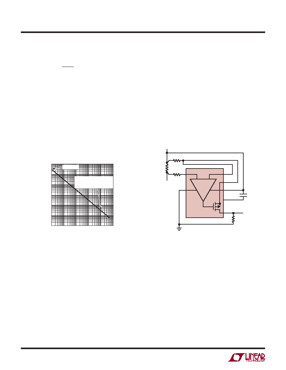
Figure 5. Second Input R Minimizes
Error Due to Input Bias Current
–INF
VREG
0.1μF
–INS
6102 F05
RIN
+ = RIN– – RSENSE
LTC6102
ROUT
VOUT
V+
LOAD
RSENSE
–
+
V+
V–
OUT
+IN
RIN
–
RIN
+
APPLICATIONS INFORMATION
For instance if IBIAS is 1nA and ROUT is 10k, the output
error is –10μV.
Note that in applications where RSENSE ≈ RIN, IB(+) causes
a voltage offset in RSENSE that cancels the error due to
IB(–) and EOUT(IBIAS) ≈ 0. In applications where RSENSE <
RIN, the bias current error can be similarly reduced if an
external resistor RIN(+) = (RIN – RSENSE) is connected as
shown in Figure 5. Under both conditions:
EOUT(IBIAS) = ± ROUT IOS; IOS = IB(+) – IB(–)
Adding RIN+ as described will maximize the dynamic
range of the circuit. For less sensitive designs, RIN+ is
not necessary.
Ideally, the circuit output is:
VV
R
VR
I
OUT
SENSE
OUT
IN
SENSE
==
;
In this case, the only error is due to resistor mismatch,
which provides an error in gain only.
Output Error, EOUT, Due to the Amplier DC Offset
Voltage, VOS
EOUT(VOS) = VOS (ROUT/RIN)
The DC offset voltage of the amplier adds directly to
the value of the sense voltage, VSENSE. This error is very
small (3μV typ) and may be ignored for reasonable values
of RIN. See Figure 4. For very high dynamic range, this
offset can be calibrated in the system due to its extremely
low drift.
INPUT VOLTAGE (V)
OUTPUT
ERROR
(%)
100
10
1
0.1
0.01
0.001
0.0001
6102 F04
0.00001 0.0001
0.001
0.01
0.1
1
FOR A 500
SHUNT
VIN = 100mV, ISHUNT = 200A
ERROR DUE TO VOS IS 6mA
VIN = 10 V
Figure 4. LTC6102 Output Error Due to Typical Input Offset
vs Input Voltage
Output Error, EOUT, Due to the Bias Currents,
IB(+) and IB(–)
The input bias current of the LTC6102 is vanishingly small.
However, for very high resolution, or at high temperatures
where IB increases due to leakage, the current may be
signicant.
The bias current IB(+) ows into the positive input of the
internal op amp. IB(–) ows into the negative input.
EOUT(IBIAS) = ROUT((IB(+) (RSENSE/RIN) – IB(–))
Since IB(+) ≈ IB(–) = IBIAS, if RSENSE << RIN then,
EOUT(IBIAS) ≈ –ROUT IBIAS
Clock Feedthrough, Input Bias Current
The LTC6102 uses auto-zeroing circuitry to achieve an
almost zero DC offset over temperature, sense voltage,
and power supply voltage. The frequency of the clock
used for auto-zeroing is typically 10kHz. The term clock
feedthrough is broadly used to indicate visibility of this
clock frequency in the op amp output spectrum. There are
typically two types of clock feedthrough in auto zeroed
amps like the LTC6102.
The rst form of clock feedthrough is caused by the
settling of the internal sampling capacitor and is input
referred; that is, it is multiplied by the internal loop gain
相关PDF资料 |
PDF描述 |
|---|---|
| LW005C | DC-DC REG PWR SUPPLY MODULE |
| LCD15-48D12W | 2-OUTPUT 15 W DC-DC REG PWR SUPPLY MODULE |
| LM2575S-ADJ | 3.2 A SWITCHING REGULATOR, 62 kHz SWITCHING FREQ-MAX, PSSO5 |
| LS1501-9EPD4TB1 | 1-OUTPUT 100 W AC-DC REG PWR SUPPLY MODULE |
| LS2320-7EPD3T | 2-OUTPUT 100 W AC-DC REG PWR SUPPLY MODULE |
相关代理商/技术参数 |
参数描述 |
|---|---|
| LTC6102HDD-PBF | 制造商:LINER 制造商全称:Linear Technology 功能描述:Precision Zero Drift Current Sense Amplifi er |
| LTC6102HDD-TR | 制造商:LINER 制造商全称:Linear Technology 功能描述:Precision Zero Drift Current Sense Amplifi er |
| LTC6102HDD-TRPBF | 制造商:LINER 制造商全称:Linear Technology 功能描述:Precision Zero Drift Current Sense Amplifi er |
| LTC6102HMS#PBF | 制造商:Linear Technology 功能描述:AMP CURRENT SENSE PRECISION SMD |
| LTC6102HMS8 | 制造商:Linear Technology 功能描述:SP Amp Current Sense Amp Single 60V 8-Pin MSOP |
发布紧急采购,3分钟左右您将得到回复。