- 您现在的位置:买卖IC网 > PDF目录44998 > LTC6102HDD-1#TRPBF (LINEAR TECHNOLOGY CORP) SPECIALTY ANALOG CIRCUIT, PDSO8 PDF资料下载
参数资料
| 型号: | LTC6102HDD-1#TRPBF |
| 厂商: | LINEAR TECHNOLOGY CORP |
| 元件分类: | 模拟信号调理 |
| 英文描述: | SPECIALTY ANALOG CIRCUIT, PDSO8 |
| 封装: | 3 X 3 MM, LEAD FREE, PLASTIC, MO-229WEED-1, DFN-8 |
| 文件页数: | 11/24页 |
| 文件大小: | 277K |
| 代理商: | LTC6102HDD-1#TRPBF |
LTC6102
LTC6102-1/LTC6102HV
19
6102fc
APPLICATIONS INFORMATION
–INF
VREG
0.1μF
–INS
6102 F11
RIN
+ = RIN– – RSENSE
LTC6102-1
ROUT
VOUT
V+
LOAD
RBIAS
2.7M
RSENSE
V+
V–
OUT
+IN
EN
RIN
–
RIN
+
–
+
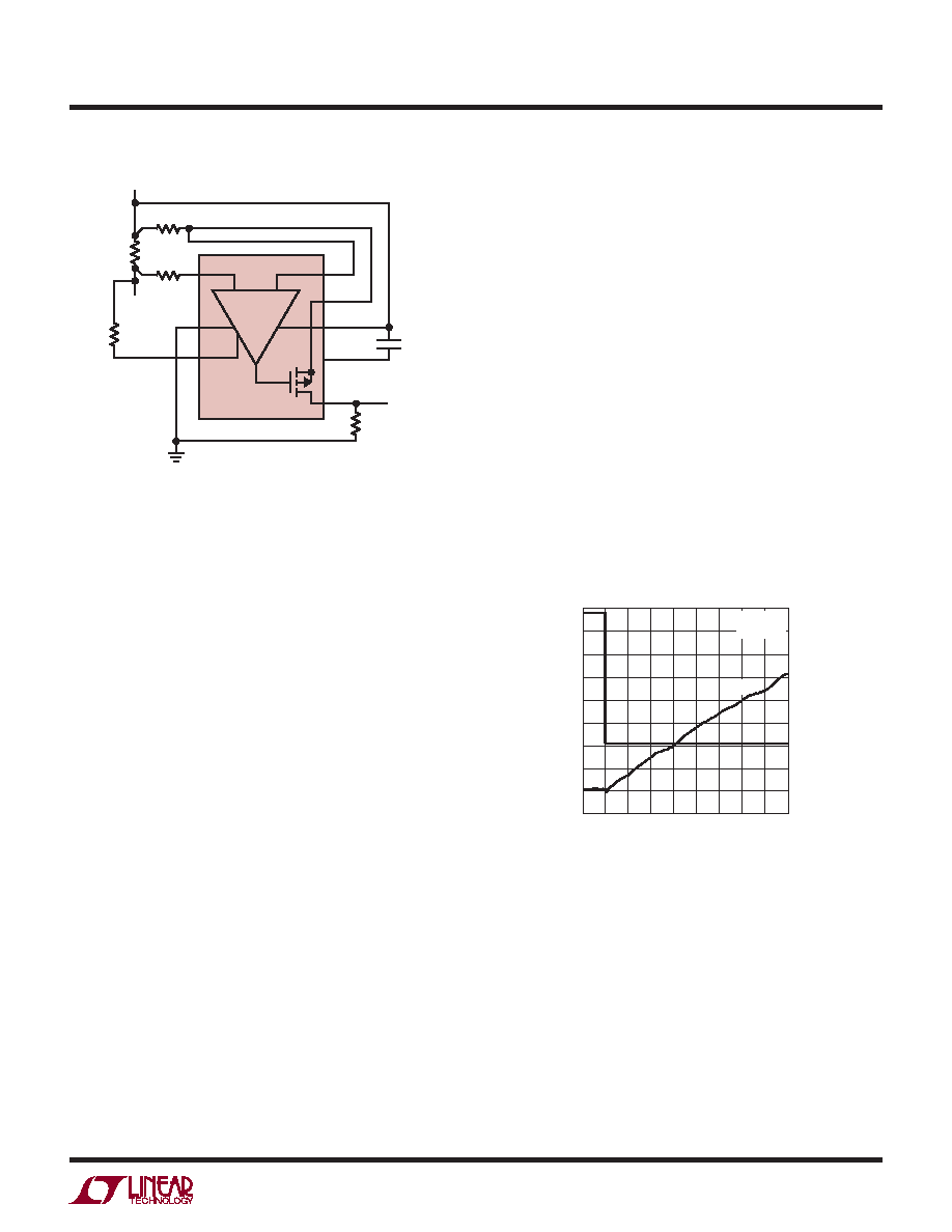
Figure 11
Figure 12. LTC6102-1 VREG Voltage During
Bypass Capacitor Discharge when Disabled
pin. Figure 11 shows the LTC6102-1 with a 2.7M pull-up
resistor to limit the current to less than 20μA with a 60V
supply, which is enough to satisfy the input bias current
requirement.
Start-Up Current
The start-up current of the LTC6102 when the part is
powered on or enabled (LTC6102-1) consists of three
parts: the rst is the current necessary to charge the
VREG bypass capacitor, which is nominally 0.1μF. Since the
VREG voltage charges to approximately 4.5V below the V+
voltage, this can require a signicant amount of start-up
current. The second source is the active supply current of
the LTC6102 amplier, which is not signicantly greater
during start-up than during normal operation. The third
source is the output current of the LTC6102, which upon
start-up may temporarily drive the output high. This could
cause milliamps of output current (limited mostly by the
input resistor RIN) to ow into the output resistor and/or
the output limiting ESD structure in the LTC6102. This is
a temporary condition which will cease when the LTC6102
amplier settles into normal closed-loop operation.
When the LTC6102-1 is disabled, the internal amplier is
also shut down, which means that the discharge rate of
the 0.1μF capacitor is very low. This is signicant when the
LTC6102-1 is disabled to save power, because the recharg-
ing of the 0.1μF capacitor is a signicant portion of the
overall power consumed in startup. Figure 12 shows the
discharge rate of the 0.1μF capacitor after the LTC6102-1
is shut down at room temperature.
In a system where the LTC6102-1 is disabled for short
periods, the start-up power (and therefore the average
power) can be reduced since the VREG bypass capacitor
is never signicantly discharged. The time required to
charge the VREG capacitor will also be reduced, allowing
the LTC6102-1 to start-up more quickly.
TIME (ms)
–2
0
ENABLE
VOL
TAGE
(V)
V
REG
VOL
TAGE
(V)
0.25
0.75
1.00
1.25
10
2.25
6102 F12
0.50
4
0
12
6
2
14
816
1.50
1.75
2.00
7.4
7.5
7.7
7.8
7.9
8.3
7.6
8.0
8.1
8.2
VREG
EN
TA = 25°C
V+ = 12V
相关PDF资料 |
PDF描述 |
|---|---|
| LTC6102HMS8-1#PBF | SPECIALTY ANALOG CIRCUIT, PDSO8 |
| LTC6102HVIDD#TR | SPECIALTY ANALOG CIRCUIT, PDSO8 |
| LTC6102HMS8-1 | SPECIALTY ANALOG CIRCUIT, PDSO8 |
| LTC6102IDD-1 | SPECIALTY ANALOG CIRCUIT, PDSO8 |
| LTC6102HVHDD | SPECIALTY ANALOG CIRCUIT, PDSO8 |
相关代理商/技术参数 |
参数描述 |
|---|---|
| LTC6102HDD-PBF | 制造商:LINER 制造商全称:Linear Technology 功能描述:Precision Zero Drift Current Sense Amplifi er |
| LTC6102HDD-TR | 制造商:LINER 制造商全称:Linear Technology 功能描述:Precision Zero Drift Current Sense Amplifi er |
| LTC6102HDD-TRPBF | 制造商:LINER 制造商全称:Linear Technology 功能描述:Precision Zero Drift Current Sense Amplifi er |
| LTC6102HMS#PBF | 制造商:Linear Technology 功能描述:AMP CURRENT SENSE PRECISION SMD |
| LTC6102HMS8 | 制造商:Linear Technology 功能描述:SP Amp Current Sense Amp Single 60V 8-Pin MSOP |
发布紧急采购,3分钟左右您将得到回复。