参数资料
| 型号: | LTC6102HDD#PBF |
| 厂商: | Linear Technology |
| 文件页数: | 10/26页 |
| 文件大小: | 0K |
| 描述: | IC AMP CURRENT SENSE 8-DFN |
| 标准包装: | 121 |
| 放大器类型: | 电流检测 |
| 电路数: | 1 |
| 增益带宽积: | 200kHz |
| 电流 - 输入偏压: | 60pA |
| 电压 - 输入偏移: | 3µV |
| 电流 - 电源: | 420µA |
| 电流 - 输出 / 通道: | 1mA |
| 电压 - 电源,单路/双路(±): | 4 V ~ 60 V |
| 工作温度: | -40°C ~ 125°C |
| 安装类型: | 表面贴装 |
| 封装/外壳: | 8-WFDFN 裸露焊盘 |
| 供应商设备封装: | 8-DFN-EP(3x3) |
| 包装: | 管件 |
| 产品目录页面: | 1322 (CN2011-ZH PDF) |
LTC6102
LTC6102-1/LTC6102HV
18
6102fd
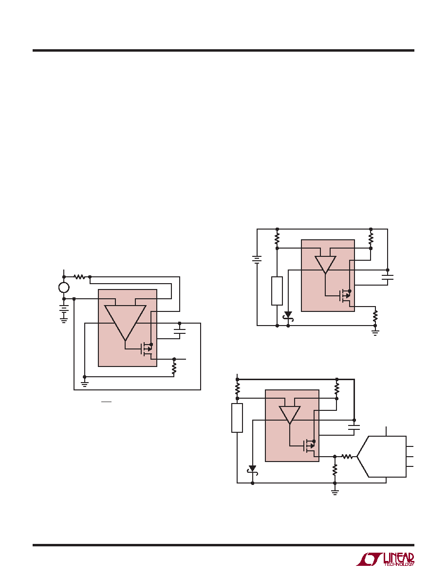
Figure 10. Additional Resistor R3 Protects
Output During Supply Reversal
APPLICATIONS INFORMATION
6102 F10
LTC6102
R2
4.99k
D1
R1
100Ω
RSENSE
–
+
V+
V–
OUT
+IN
VBATT
R3
1k
–INF
–INS
VREG
0.1μF
L
O
A
D
ADC
the allowed output current. The gain is still controlled by
ROUT/RIN, so either gain or attenuation may be applied to
the input signal as it is translated to the output. Finally,
the input may be a voltage source rather than a sense
resistor, as shown in Figure 8. This circuit allows the
translation of a wide variety of input signals across the
entire supply range of the LTC6102 with only a tiny offset
error while retaining simple gain control set by ROUT/RIN.
Again, very large voltages may be sensed as long as RIN
is chosen so that IOUT does not exceed the allowed output
current. For example, VIN may be as large as 1V with RIN =
1k, or as large as 10V with RIN = 10k. For a 10V maximum
input and a 5V maximum output, RIN = 10k and ROUT = 5k
will allow the LTC6102HV to translate VIN to VOUT with a
common mode voltage of up to 100V. For the case where
a large input resistor is used, a similar resistor in series
with +IN will reduce error due to input bias current.
Figure 8. Voltage Level-Shift Circuit
Figure 9. Schottky Prevents Damage During Supply Reversal
–INF
–INS
LTC6102
ROUT
VOUT
6102 F08
RIN
VIN
VCM
V+
V–
OUT
+IN
VREG
0.1μF
–
+
VOUT = VIN
ROUT
RIN
6102 F09
LTC6102
R2
4.99k
D1
R1
100Ω
VBATT
RSENSE
V+
V–
–INF
OUT
–INS
+IN
VREG
0.1μF
L
O
A
D
–
+
Reverse Supply Current
Some applications may be tested with reverse-polarity
supplies due to an expectation of this type of fault during
operation. The LTC6102 is not protected internally from
external reversal of supply polarity. To prevent damage
that may occur during this condition, a Schottky diode
should be added in series with V– (Figure 9). This will
limit the reverse current through the LTC6102. Note that
this diode will limit the low voltage performance of the
LTC6102 by effectively reducing the supply voltage to the
part by VD.
In addition, if the output of the LTC6102 is wired to a device
that will effectively short it to high voltage (such as through
an ESD protection clamp) during a reverse supply condi-
tion, the LTC6102’s output should be connected through
a resistor or Schottky diode (Figure 10).
Response Time
The LTC6102 is designed to exhibit fast response to inputs
for the purpose of circuit protection or signal transmission.
This response time will be affected by the external circuit
in two ways, delay and speed.
相关PDF资料 |
PDF描述 |
|---|---|
| SMCJ170A | TVS UNIDIRECT 1500W 170V SMC |
| LTC6102HMS8#PBF | IC AMP CURRENT SENSE 8-MSOP |
| 929834-03-08 | CONN HEADER .100 SNGL STR 8POS |
| OP296GSZ | IC OPAMP GP R-R 450KHZ LP 8SOIC |
| AD8139ACPZ-REEL7 | IC AMP DIFF R-R LN LDIST 8LFCSP |
相关代理商/技术参数 |
参数描述 |
|---|---|
| LTC6102HDD-TR | 制造商:LINER 制造商全称:Linear Technology 功能描述:Precision Zero Drift Current Sense Amplifi er |
| LTC6102HDD-TRPBF | 制造商:LINER 制造商全称:Linear Technology 功能描述:Precision Zero Drift Current Sense Amplifi er |
| LTC6102HMS#PBF | 制造商:Linear Technology 功能描述:AMP CURRENT SENSE PRECISION SMD |
| LTC6102HMS8 | 制造商:Linear Technology 功能描述:SP Amp Current Sense Amp Single 60V 8-Pin MSOP |
| LTC6102HMS8#PBF | 功能描述:IC AMP CURRENT SENSE 8-MSOP RoHS:是 类别:集成电路 (IC) >> Linear - Amplifiers - Instrumentation 系列:- 标准包装:2,500 系列:- 放大器类型:通用 电路数:4 输出类型:- 转换速率:0.6 V/µs 增益带宽积:1MHz -3db带宽:- 电流 - 输入偏压:45nA 电压 - 输入偏移:2000µV 电流 - 电源:1.4mA 电流 - 输出 / 通道:40mA 电压 - 电源,单路/双路(±):3 V ~ 32 V,±1.5 V ~ 16 V 工作温度:0°C ~ 70°C 安装类型:表面贴装 封装/外壳:14-TSSOP(0.173",4.40mm 宽) 供应商设备封装:14-TSSOP 包装:带卷 (TR) 其它名称:LM324ADTBR2G-NDLM324ADTBR2GOSTR |
发布紧急采购,3分钟左右您将得到回复。