- 您现在的位置:买卖IC网 > PDF目录98003 > LTC6103CMS8#TR (LINEAR TECHNOLOGY CORP) 2-CHANNEL POWER SUPPLY SUPPORT CKT, PDSO8 PDF资料下载
参数资料
| 型号: | LTC6103CMS8#TR |
| 厂商: | LINEAR TECHNOLOGY CORP |
| 元件分类: | 电源管理 |
| 英文描述: | 2-CHANNEL POWER SUPPLY SUPPORT CKT, PDSO8 |
| 封装: | PLASTIC, MSOP-8 |
| 文件页数: | 2/16页 |
| 文件大小: | 264K |
| 代理商: | LTC6103CMS8#TR |
LTC6103
10
6103f
Error Sources
The current sense system uses an amplier and resistors
to apply gain and level shift the result. The output is then
dependent on the characteristics of the amplier, such as
bias current and input offset, as well as resistor matching.
Ideally, the circuit output is:
VV
R
VR
I
OUT
SENSE
OUT
IN
SENSE
=
In this case, the only error is due to resistor mismatch,
which provides an error in gain only. However, offset
voltage, bias current and nite gain in the amplier cause
additional errors.
Output Error, EOUT, Due to the Amplier DC Offset
Voltage, VOS
EV
R
OUT VOS
OS
OUT
IN
()
=
The DC offset voltage of the amplier adds directly to the
value of the sense voltage, VSENSE. This is the dominant
error of the system and it limits the available dynamic
range. The paragraph, Selection of External Current Sense
Resistor provides details.
Output Error, EOUT, Due to Bias Currents
The bias current IB(+) ows into the positive input of the
internal op amp. IB(–) ows into the negative input.
EOUT(IBIAS) = ROUT(IB(+) (RSENSE/RIN) – IB(–))
Since IB(+) ≈ IB(–) = IBIAS, if RSENSE << RIN then:
EOUT(IBIAS) ≈ –ROUT IBIAS
For instance, if IBIAS is 100nA and ROUT is 1k, then the
output error is 0.1mV.
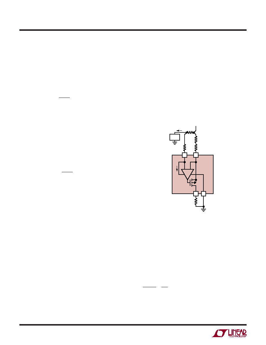
Output Error, EOUT, Due to PCB Trace Resistance
The LTC6103 uses the +IN pin for both the positive amplier
input and the positive supply input for the amplier. The
supply current can cause an output error if trace resistance
between RSENSE and +IN is signicant (Figure 4).
EOUT(RT_+IN) = (IS RT/RIN) ROUT
Trace resistance to the –IN pin will increase the effective
RIN value, causing a gain error. In addition, internal device
resistance will add approximately 0.3
Ω to RIN.
Minimizing the trace resistance is important and care
should be taken in the PCB layout. Make the trace short
and wide. Kelvin connection to the shunt resistor pad
should be used.
APPLICATIONS INFORMATION
Figure 4. Error Due to PCB Trace Resistance
+
–
+IN
OUT
VS
IS
1/2
LTC6103
–IN
RIN
RT
RSENSE
V+
V–
ROUT
6103 F04
LOAD
ILOAD
Output Error, EOUT, Due to the Finite DC Open-Loop Gain,
AOL, of the LTC6103 Amplier
This error is inconsequential as the AOL of the LTC6103
is very large.
Design Example:
If ISENSE range = (1A to 1mA) and:
V
I
V
A
OUT
SENSE
=
3
1
相关PDF资料 |
PDF描述 |
|---|---|
| LTC6103HMS8#TR | 2-CHANNEL POWER SUPPLY SUPPORT CKT, PDSO8 |
| LTC6604CUFF-10#TRPBF | SPECIALTY ANALOG CIRCUIT, PQCC34 |
| LUC025F | 2-OUTPUT 16.5 W DC-DC REG PWR SUPPLY MODULE |
| LV56801P | 1-CHANNEL POWER SUPPLY SUPPORT CKT, ZIP15 |
| LV5693P | 6-CHANNEL POWER SUPPLY SUPPORT CKT, PZFM15 |
相关代理商/技术参数 |
参数描述 |
|---|---|
| LTC6103HMS8 | 制造商:LINER 制造商全称:Linear Technology 功能描述:Dual High Voltage, High Side Current Sense Amplifier |
| LTC6103HMS8#PBF | 功能描述:IC AMP CURRENT SENSE 8-MSOP RoHS:是 类别:集成电路 (IC) >> Linear - Amplifiers - Instrumentation 系列:- 产品培训模块:Differential Circuit Design Techniques for Communication Applications 标准包装:1 系列:- 放大器类型:RF/IF 差分 电路数:1 输出类型:差分 转换速率:9800 V/µs 增益带宽积:- -3db带宽:2.9GHz 电流 - 输入偏压:3µA 电压 - 输入偏移:- 电流 - 电源:40mA 电流 - 输出 / 通道:- 电压 - 电源,单路/双路(±):3 V ~ 3.6 V 工作温度:-40°C ~ 85°C 安装类型:表面贴装 封装/外壳:16-VQFN 裸露焊盘,CSP 供应商设备封装:16-LFCSP-VQ 包装:剪切带 (CT) 产品目录页面:551 (CN2011-ZH PDF) 其它名称:ADL5561ACPZ-R7CT |
| LTC6103HMS8#TRPBF | 功能描述:IC AMP CURRENT SENSE 8-MSOP RoHS:是 类别:集成电路 (IC) >> Linear - Amplifiers - Instrumentation 系列:- 标准包装:1 系列:- 放大器类型:通用 电路数:4 输出类型:满摆幅 转换速率:0.6 V/µs 增益带宽积:1MHz -3db带宽:- 电流 - 输入偏压:2pA 电压 - 输入偏移:1000µV 电流 - 电源:85µA 电流 - 输出 / 通道:20mA 电压 - 电源,单路/双路(±):1.8 V ~ 6 V 工作温度:-40°C ~ 125°C 安装类型:表面贴装 封装/外壳:14-SOIC(0.154",3.90mm 宽) 供应商设备封装:14-SOICN 包装:剪切带 (CT) 产品目录页面:680 (CN2011-ZH PDF) 其它名称:MCP6L04T-E/SLCT |
| LTC6103IMS8 | 制造商:Linear Technology 功能描述:OP Amp Dual GP 60V 8-Pin MSOP |
| LTC6103IMS8#PBF | 功能描述:IC AMP CURRENT SENSE 8-MSOP RoHS:是 类别:集成电路 (IC) >> Linear - Amplifiers - Instrumentation 系列:- 产品培训模块:Differential Circuit Design Techniques for Communication Applications 标准包装:1 系列:- 放大器类型:RF/IF 差分 电路数:1 输出类型:差分 转换速率:9800 V/µs 增益带宽积:- -3db带宽:2.9GHz 电流 - 输入偏压:3µA 电压 - 输入偏移:- 电流 - 电源:40mA 电流 - 输出 / 通道:- 电压 - 电源,单路/双路(±):3 V ~ 3.6 V 工作温度:-40°C ~ 85°C 安装类型:表面贴装 封装/外壳:16-VQFN 裸露焊盘,CSP 供应商设备封装:16-LFCSP-VQ 包装:剪切带 (CT) 产品目录页面:551 (CN2011-ZH PDF) 其它名称:ADL5561ACPZ-R7CT |
发布紧急采购,3分钟左右您将得到回复。