参数资料
| 型号: | LTC6103IMS8#PBF |
| 厂商: | Linear Technology |
| 文件页数: | 13/16页 |
| 文件大小: | 0K |
| 描述: | IC AMP CURRENT SENSE 8-MSOP |
| 标准包装: | 50 |
| 放大器类型: | 电流检测 |
| 电路数: | 2 |
| 增益带宽积: | 140kHz |
| 电流 - 输入偏压: | 100nA |
| 电压 - 输入偏移: | 85µV |
| 电流 - 电源: | 390µA |
| 电流 - 输出 / 通道: | 1mA |
| 电压 - 电源,单路/双路(±): | 4 V ~ 60 V,±2 V ~ 30 V |
| 工作温度: | -40°C ~ 85°C |
| 安装类型: | 表面贴装 |
| 封装/外壳: | 8-TSSOP,8-MSOP(0.118",3.00mm 宽) |
| 供应商设备封装: | 8-MSOP |
| 包装: | 管件 |
| 产品目录页面: | 1322 (CN2011-ZH PDF) |
LTC6103
6
6103f
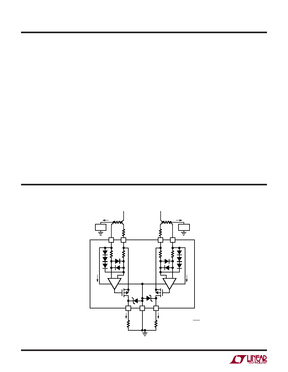
BLOCK DIAGRAM
PIN FUNCTIONS
OUTA (Pin 1): Current Output of Amplier A. OUTA will
source a current that is proportional to the sense voltage
of amplier A into an external resistor.
OUTB (Pin 2): Current Output of Amplier B. OUTB will
source a current that is proportional to the sense voltage
of amplier B into an external resistor.
NC (Pin 3): No Connect.
V– (Pin 4): Negative Supply (or Ground for Single Supply
Operation). Common to both ampliers.
+INB/VSB (Pin 5): The Positive Input of the Internal Sense
Amplier B. Must be tied to the system load end of the
sense resistor. It also works as the positive supply for
amplier B. Supply current of amplier B is drawn through
this pin. The LTC6103 supply current is monitored along
with the system load current.
–INB (Pin 6): The Negative Input of the Internal Sense
Amplier B. The internal sense amplier will drive –INB
to the same potential as +INB. A resistor (RIN) tied from
VB
+ to –INB sets the output current IOUT = VSENSE/ RIN.
VSENSE is the voltage developed across the external RSENSE
(Figure 1).
–INA (Pin 7): The Negative Input of the Internal Sense
Amplier A. The internal sense amplier will drive –INA
to the same potential as +INA. A resistor (RIN) tied from
VA
+ to –INA sets the output current IOUT = VSENSE/ RIN.
VSENSE is the voltage developed across the external RSENSE
(Figure 1).
+INA/VSA (Pin 8): The Positive Input of the Internal Sense
Amplier A. Must be tied to the system load end of the
sense resistor. It also works as the positive supply for
amplier A. Supply current of amplier A is drawn through
this pin. The LTC6103 supply current is monitored along
with the system load current.
Figure 1. LTC6103 Block Diagram and Typical Connection
+
–
+
–
8
7
6
5
2
4
1
+INA
OUTA
OUTB
6103 F01
VSB
VSA
ISA
ISB
IOUT
–INA
–INB
RIN
5k 5k
RIN
RSENSE
VSENSE
+–
VSENSE
+
–
VA
+
VB
+
+INB
V–
10V
ROUT
LOAD
ILOAD
ROUT
RIN
VOUT = VSENSE
相关PDF资料 |
PDF描述 |
|---|---|
| AWHW40-G-SMD-R | CONN HEADER LO-PRO 40POS AU SMD |
| LT6402CUD-20#PBF | IC DIFF AMP/ADC DRVR 16-QFN |
| AD8512ARZ | IC OPAMP JFET 8MHZ DUAL LN 8SOIC |
| LT1994IDD#PBF | IC DIFF AMP/DRIVER LN 8-DFN |
| LTC6244HMS8#PBF | IC OP AMP DUAL R-R 8-MSOP |
相关代理商/技术参数 |
参数描述 |
|---|---|
| LTC6104 | 制造商:LINER 制造商全称:Linear Technology 功能描述:36V Low Cost High Side Current Sense in a SOT-23 |
| LTC6104CMS8 | 制造商:LINER 制造商全称:Linear Technology 功能描述:High Voltage, High Side, Bi-Directional Current Sense Amplifi er |
| LTC6104CMS8#PBF | 功能描述:IC AMP CURRENT SENSE 8-MSOP RoHS:是 类别:集成电路 (IC) >> Linear - Amplifiers - Instrumentation 系列:- 其它有关文件:Automotive Product Guide 产品培训模块:Lead (SnPb) Finish for COTS Obsolescence Mitigation Program 标准包装:1 系列:- 放大器类型:通用 电路数:1 输出类型:满摆幅 转换速率:3 V/µs 增益带宽积:10MHz -3db带宽:- 电流 - 输入偏压:1pA 电压 - 输入偏移:70µV 电流 - 电源:2.5mA 电流 - 输出 / 通道:48mA 电压 - 电源,单路/双路(±):2.7 V ~ 5.5 V,±1.35 V ~ 2.75 V 工作温度:-40°C ~ 125°C 安装类型:表面贴装 封装/外壳:SOT-23-6 供应商设备封装:SOT-6 包装:Digi-Reel® 其它名称:MAX4475AUT#TG16DKR |
| LTC6104CMS8#TRPBF | 功能描述:IC AMP CURRENT SENSE 8-MSOP RoHS:是 类别:集成电路 (IC) >> Linear - Amplifiers - Instrumentation 系列:- 标准包装:1,000 系列:- 放大器类型:电压反馈 电路数:4 输出类型:满摆幅 转换速率:33 V/µs 增益带宽积:20MHz -3db带宽:30MHz 电流 - 输入偏压:2nA 电压 - 输入偏移:3000µV 电流 - 电源:2.5mA 电流 - 输出 / 通道:30mA 电压 - 电源,单路/双路(±):4.5 V ~ 16.5 V,±2.25 V ~ 8.25 V 工作温度:-40°C ~ 85°C 安装类型:表面贴装 封装/外壳:14-SOIC(0.154",3.90mm 宽) 供应商设备封装:14-SOIC 包装:带卷 (TR) |
| LTC6104CMS8PBF | 制造商:Linear Technology 功能描述:Bi-Directional Curr Sense Amp LTC6104 |
发布紧急采购,3分钟左右您将得到回复。