参数资料
| 型号: | LTC6104IMS8#PBF |
| 厂商: | Linear Technology |
| 文件页数: | 10/16页 |
| 文件大小: | 0K |
| 描述: | IC AMP CURRENT SENSE 8-MSOP |
| 标准包装: | 50 |
| 放大器类型: | 电流检测 |
| 电路数: | 1 |
| 增益带宽积: | 200kHz |
| 电流 - 输入偏压: | 100nA |
| 电压 - 输入偏移: | 85µV |
| 电流 - 电源: | 640µA |
| 电流 - 输出 / 通道: | 1mA |
| 电压 - 电源,单路/双路(±): | 4 V ~ 60 V,±2 V ~ 30 V |
| 工作温度: | -40°C ~ 85°C |
| 安装类型: | 表面贴装 |
| 封装/外壳: | 8-TSSOP,8-MSOP(0.118",3.00mm 宽) |
| 供应商设备封装: | 8-MSOP |
| 包装: | 管件 |
| 产品目录页面: | 1322 (CN2011-ZH PDF) |
LTC6104
3
6104f
Note 1: Stresses beyond those listed under Absolute Maximum Ratings
may cause permanent damage to the device. Exposure to any Absolute
Maximum Rating condition for extended periods may affect device
reliability and lifetime.
Note 2: The LTC6104C is guaranteed to meet specied performance from
0°C to 70°C. The LTC6104C is designed, characterized and expected to
meet specied performance from –40°C to 85°C but are not tested or QA
sampled at these temperatures. LTC6104I is guaranteed to meet specied
performance from –40°C to 85°C. The LTC6104H is guaranteed to meet
specied performance from –40°C to 125°C.
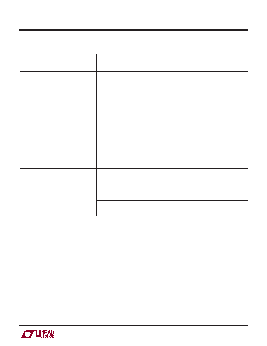
ELECTRICAL CHARACTERISTICS The ● denotes the specications which apply over the full operating
temperature range, otherwise specications are at TA = 25°C. RIN = 100Ω, ROUT = 5k, 4V ≤ +INB(VS) ≤ 60V, V
– = 0V, VREF = 2V for
VS ≥ 6V, VREF = 0.75V for VS = 4V, unless otherwise noted.
SYMBOL
PARAMETER
CONDITIONS
MIN
TYP
MAX
UNITS
IOUT(MAX)
Maximum Output Current
6V ≤ VS ≤ 60V, VSENSE = ±110mV, VREF = 2V, ROUT = 1k
VS = 4V, VSENSE = ±27.5mV, VREF = 0.75V, ROUT = 1k
●
±1
±0.25
mA
IOUT-GAINERR Current Mirror Gain Error
VINB
– > VINB+ and VINA– < VINA+ (Note 4)
±0.2
±0.75
%
IOUT-OSERR
Current Mirror Offset Error
VINB
– > VINB+ and VINA– < VINA+ (Note 4)
±0.2
A
tr
Input Step Response (
ΔVOUT = to
50% on a 5V Output Step)
8V ≤ VS ≤ 60V, VREF = 1V, VSENSE = 0mV to 100mV
Transient
1s
8V ≤ VS ≤ 60V, VREF = 6V, VSENSE = –100mV to 0mV
Transient
1s
8V ≤ VS ≤ 60V, VREF = 4V, VSENSE = –50mV to 50mV
Transient
3s
Input Step Response (
ΔVOUT = to
50% on a 0.5V Output Step)
VS = 4V, ROUT = 500Ω, Gain = 5, VREF = 0.5V,
VSENSE = 0mV to 100mV Transient
1.2
s
VS = 4V, ROUT = 500Ω, Gain = 5, VREF = 1V,
VSENSE = –100mV to 0mV Transient
1.2
s
VS = 4V, ROUT = 500Ω, Gain = 5, VREF = 0.75V,
VSENSE = –50mV to 50mV Transient
3.2
s
BW
Signal Bandwidth
IOUT = 200A, ROUT = 5k
IOUT = –200A, ROUT = 5k
IOUT = 1mA, ROUT = 5k
IOUT = –1mA, ROUT = 5k
140
200
kHz
IS
Supply Current
VS = 4V, IOUT = 0, RIN = 1M
●
0.45
0.73
0.825
mA
VS = 6V, IOUT = 0, RIN = 1M
●
0.5
0.79
1
mA
VS = 12V, IOUT = 0, RIN = 1M
●
0.52
0.81
1
mA
VS = 60V, IOUT = 0, RIN = 1M
LTC6104I, LTC6104C
LTC6104H
●
0.64
1.04
1.1
1.2
mA
Note 3: VSENSE(MAX) is tested by applying 550mV and verifying the gain
error is less than 1%. The 1% limit is set by the accuracy of high speed
test equipment. Gain error is typically dominated by external resistor
tolerance.
Note 4: When amplier A is active and amplier B is inactive, the gain
error is entirely due to the external resistors RIN and ROUT. When amplier
A is inactive and amplier B is active, there is an additional gain error from
the LTC6104 current mirror circuit. This error term is the gain error term,
IOUT-GAINERR plus the offset error term, IOUT-OSERR.
相关PDF资料 |
PDF描述 |
|---|---|
| 76382-312LF | CONN HEADER 12POS .100" R/A GOLD |
| SBH31-NBPB-D07-SP-BK | CONN HDR 1.27MM 14POS GOLD SMD |
| 68015-436HLF | BERGSTIK II .100" SR R/A |
| AD8203YRZ | IC AMP DIFF 60KHZ 8SOIC |
| ADA4001-2ARZ | IC OPAMP JFET R-R DUAL 8SOIC |
相关代理商/技术参数 |
参数描述 |
|---|---|
| LTC612A1G | 制造商:未知厂家 制造商全称:未知厂家 功能描述:Optoelectronic |
| LTC612A1P | 制造商:未知厂家 制造商全称:未知厂家 功能描述:Optoelectronic |
| LTC612D1G | 制造商:未知厂家 制造商全称:未知厂家 功能描述:Optoelectronic |
| LTC612D1P | 制造商:未知厂家 制造商全称:未知厂家 功能描述:Optoelectronic |
| LTC617A1G | 制造商:未知厂家 制造商全称:未知厂家 功能描述:Optoelectronic |
发布紧急采购,3分钟左右您将得到回复。