参数资料
| 型号: | LTC6244HVIMS8#TRPBF |
| 厂商: | Linear Technology |
| 文件页数: | 9/26页 |
| 文件大小: | 0K |
| 描述: | IC OP AMP DUAL R-R 8-MSOP |
| 标准包装: | 2,500 |
| 放大器类型: | 通用 |
| 电路数: | 2 |
| 输出类型: | 满摆幅 |
| 转换速率: | 40 V/µs |
| 增益带宽积: | 50MHz |
| 电流 - 输入偏压: | 1pA |
| 电压 - 输入偏移: | 50µV |
| 电流 - 电源: | 7mA |
| 电流 - 输出 / 通道: | 55mA |
| 电压 - 电源,单路/双路(±): | 2.8 V ~ 11 V,±1.4 V ~ 5.5 V |
| 工作温度: | -40°C ~ 85°C |
| 安装类型: | 表面贴装 |
| 封装/外壳: | 8-TSSOP,8-MSOP(0.118",3.00mm 宽) |
| 供应商设备封装: | 8-MSOP |
| 包装: | 带卷 (TR) |
LTC6244
17
6244fb
Large Area Photodiode Ampliers
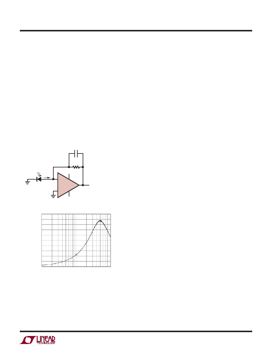
A simple large area photodiode amplier is shown in
Figure 4a. The capacitance of the photodiode is 3650pF
(nominally 3000pF), and this has a signicant effect on
the noise performance of the circuit. For example, the
photodiode capacitance at 10kHz equates to an impedance
of 4.36kΩ, so the op amp circuit with 1MΩ feedback has a
noise gain of NG = 1 + 1M/4.36k = 230 at that frequency.
Therefore, the LTC6244 input voltage noise gets to the
output as NG 7.8nV/√Hz = 1800nV/√Hz, and this can
clearly be seen in the circuit’s output noise spectrum in
Figure 4b. Note that we have not yet accounted for the
op amp current noise, or for the 130nV/√Hz of the gain
resistor, but these are obviously trivial compared to the op
amp voltage noise and the noise gain. For reference, the
DC output offset of this circuit is about 100μV, bandwidth
is 52kHz, and the total noise was measured at 1.7mVRMS
on a 100kHz measurement bandwidth.
An improvement to this circuit is shown in Figure 5a,
where the large diode capacitance is bootstrapped by a
1nV/√Hz JFET. This depletion JFET has a VGS of about
–0.5V, so that RBIAS forces it to operate at just over 1mA of
drain current. Connected as shown, the photodiode has a
reverse bias of one VGS, so its capacitance will be slightly
lower than in the previous case (measured 2640pF), but
the most drastic effects are due to the bootstrapping.
Figure 5b shows the output noise of the new circuit.
Noise at 10kHz is now 220nV/√Hz, and the 130nV/√Hz
noise thermal noise oor of the 1M feedback resistor
is discernible at low frequencies. What has happened is
that the 7.8nV/√Hz of the op amp has been effectively
replaced by the 1nV/√Hz of the JFET. This is because the
1M feedback resistor is no longer “looking back” into the
large photodiode capacitance. It is instead looking back
into a JFET gate capacitance, an op amp input capacitance,
and some parasitics, approximately 10pF total. The large
photodiode capacitance is across the gate-source volt-
age of the low noise JFET. Doing a sample calculation at
10kHz as before, the photodiode capacitance looks like
6kΩ, so the 1nV/√Hz of the JFET creates a current noise
of 1nV/6k = 167fA/√Hz. This current noise necessarily
ows through the 1M feedback resistor, and so appears
as 167nV/√Hz at the output. Adding the 130nV/√Hz of the
resistor (RMS wise) gives a total calculated noise density
of 210nV/√Hz, agreeing well with the measured noise of
Figure 5b. Another drastic improvement is in bandwidth,
now over 350kHz, as the bootstrap enabled a reduction
of the compensating feedback capacitance. Note that the
bootstrap does not affect the DC accuracy of the amplier,
except by adding a few picoamps of gate current.
There is one drawback to this circuit. Most photodiode
circuits require the ability to set the amount of applied
reverse bias, whether it’s 0V, 5V, or 200V. This circuit has
a xed reverse bias of about 0.5V, dictated by the JFET.
Figure 4b. Output Noise Spectral Density of the Circuit of Figure
4a. At 10kHz, the 1800nV/√Hz Output Noise is Due Almost
Entirely to the 7.8nV Voltage Noise of the LTC6244 and the High
Noise Gain of the 1M Feedback Resistor Looking Into the High
Photodiode Capacitance
Figure 4a. Large Area Photodiode Transimpedance Amplier
APPLICATIONS INFORMATION
5V
VOUT = 1M IPD
BW = 52kHz
NOISE = 1800nV/√Hz AT 10kHz
IPD
RF
1M
HAMAMATSU
LARGE AREA
PHOTODIODE
S1227-1010BQ
CPD = 3000pF
CF
3.9pF
–5V 6244 F04a
–
+
1/2
LTC6244HV
VOUT
1k
10k
FREQUENCY (Hz)
6244 F04b
100k
OUTPUT
NOISE
(800nV/√
Hz
/DIV)
相关PDF资料 |
PDF描述 |
|---|---|
| RC0805FR-072R55L | RES 2.55 OHM 1/8W 1% 0805 SMD |
| XT800C | GAS TRIGGER TUBE 800V CORE |
| XT600C | GAS TRIGGER TUBE 600V CORE |
| XT350C | GAS TRIGGER TUBE 350V CORE |
| RC0805FR-072R1L | RES 2.10 OHM 1/8W 1% 0805 SMD |
相关代理商/技术参数 |
参数描述 |
|---|---|
| LTC6244IDD | 制造商:LINER 制造商全称:Linear Technology 功能描述:Dual 50MHz, Low Noise, Rail-to-Rail, CMOS Op Amp |
| LTC6244IDD#PBF | 功能描述:IC OP AMP DUAL R-R 8-DFN RoHS:是 类别:集成电路 (IC) >> Linear - Amplifiers - Instrumentation 系列:- 产品培训模块:Differential Circuit Design Techniques for Communication Applications 标准包装:1 系列:- 放大器类型:RF/IF 差分 电路数:1 输出类型:差分 转换速率:9800 V/µs 增益带宽积:- -3db带宽:2.9GHz 电流 - 输入偏压:3µA 电压 - 输入偏移:- 电流 - 电源:40mA 电流 - 输出 / 通道:- 电压 - 电源,单路/双路(±):3 V ~ 3.6 V 工作温度:-40°C ~ 85°C 安装类型:表面贴装 封装/外壳:16-VQFN 裸露焊盘,CSP 供应商设备封装:16-LFCSP-VQ 包装:剪切带 (CT) 产品目录页面:551 (CN2011-ZH PDF) 其它名称:ADL5561ACPZ-R7CT |
| LTC6244IDD#TRPBF | 功能描述:IC OP AMP DUAL R-R 8-DFN RoHS:是 类别:集成电路 (IC) >> Linear - Amplifiers - Instrumentation 系列:- 标准包装:50 系列:- 放大器类型:通用 电路数:2 输出类型:满摆幅 转换速率:1.8 V/µs 增益带宽积:6.5MHz -3db带宽:4.5MHz 电流 - 输入偏压:5nA 电压 - 输入偏移:100µV 电流 - 电源:65µA 电流 - 输出 / 通道:35mA 电压 - 电源,单路/双路(±):1.8 V ~ 5.25 V,±0.9 V ~ 2.625 V 工作温度:-40°C ~ 85°C 安装类型:表面贴装 封装/外壳:10-TFSOP,10-MSOP(0.118",3.00mm 宽) 供应商设备封装:10-MSOP 包装:管件 |
| LTC6244IMS8 | 制造商:LINER 制造商全称:Linear Technology 功能描述:Dual 50MHz, Low Noise, Rail-to-Rail, CMOS Op Amp |
| LTC6244IMS8#PBF | 功能描述:IC OP AMP DUAL R-R 8-MSOP RoHS:是 类别:集成电路 (IC) >> Linear - Amplifiers - Instrumentation 系列:- 产品培训模块:Differential Circuit Design Techniques for Communication Applications 标准包装:1 系列:- 放大器类型:RF/IF 差分 电路数:1 输出类型:差分 转换速率:9800 V/µs 增益带宽积:- -3db带宽:2.9GHz 电流 - 输入偏压:3µA 电压 - 输入偏移:- 电流 - 电源:40mA 电流 - 输出 / 通道:- 电压 - 电源,单路/双路(±):3 V ~ 3.6 V 工作温度:-40°C ~ 85°C 安装类型:表面贴装 封装/外壳:16-VQFN 裸露焊盘,CSP 供应商设备封装:16-LFCSP-VQ 包装:剪切带 (CT) 产品目录页面:551 (CN2011-ZH PDF) 其它名称:ADL5561ACPZ-R7CT |
发布紧急采购,3分钟左右您将得到回复。