参数资料
| 型号: | LTC6253CDC#TRMPBF |
| 厂商: | Linear Technology |
| 文件页数: | 7/26页 |
| 文件大小: | 0K |
| 描述: | IC OPAMP R-R 720MHZ DFN-8 |
| 标准包装: | 1 |
| 放大器类型: | 通用 |
| 电路数: | 2 |
| 输出类型: | 满摆幅 |
| 转换速率: | 280 V/µs |
| 增益带宽积: | 720MHz |
| -3db带宽: | 400MHz |
| 电流 - 输入偏压: | 1.4µA |
| 电压 - 输入偏移: | 100µV |
| 电流 - 电源: | 4.25mA |
| 电流 - 输出 / 通道: | 100mA |
| 电压 - 电源,单路/双路(±): | 2.5 V ~ 5.25 V,±1.25 V ~ 2.625 V |
| 工作温度: | 0°C ~ 70°C |
| 安装类型: | 表面贴装 |
| 封装/外壳: | 8-WFDFN 裸露焊盘 |
| 供应商设备封装: | 8-DFN-EP(2x2) |
| 包装: | 标准包装 |
| 其它名称: | LTC6253CDC#TRMPBFDKR |
LTC6252/LTC6253/LTC6254
15
625234fc
APPLICATIONS INFORMATION
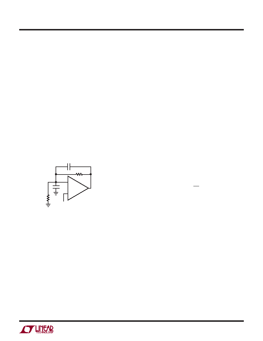
Figure 2. 5pF Feedback Cancels Parasitic Pole
Feedback Components
When feedback resistors are used to set up gain, care
must be taken to ensure that the pole formed by the
feedback resistors and the parasitic capacitance at the
inverting input does not degrade stability. For example
if the amplifier is set up in a gain of +2 configuration
with gain and feedback resistors of 5k, a parasitic ca-
pacitance of 5pF (device + PC board) at the amplifier’s
inverting input will cause the part to oscillate, due to
a pole formed at 12.7MHz. An additional capacitor of
5pF across the feedback resistor as shown in Figure 2
will eliminate any ringing or oscillation. In general, if
the resistive feedback network results in a pole whose
frequency lies within the closed loop bandwidth of the
amplifier, a capacitor can be added in parallel with the
feedback resistor to introduce a zero whose frequency
is close to the frequency of the pole, improving stability.
624678 F02
CPAR
5k
–
+
VOUT
VIN
5k
5pF
Power Dissipation
The LTC6252 and LTC6253 contain one and two amplifiers
respectively. Hence the maximum on-chip power dissipa-
tion for them will be less than the maximum on-chip power
dissipationfortheLTC6254,whichcontainsfouramplifiers.
The LTC6254 is housed in a small 16-lead MS package and
typically has a thermal resistance (
qJA) of 125°C/ W. It is
necessary to ensure that the die’s junction temperature
does not exceed 150°C. The junction temperature, TJ, is
calculated from the ambient temperature, TA, power dis-
sipation, PD, and thermal resistance,
qJA:
TJ = TA + (PD qJA)
The power dissipation in the IC is a function of the supply
voltage, output voltage and load resistance. For a given
supply voltage with output connected to ground or supply,
the worst-case power dissipation PD(MAX) occurs when
the supply current is maximum and the output voltage at
half of either supply voltage for a given load resistance.
PD(MAX) is approximately (since IS actually changes with
output load current) given by:
PD(MAX) =(VS IS(MAX))+
VS
2
2
/ RL
Example:ForanLTC6254ina16-leadMSpackageoperating
on ±2.5V supplies and driving a 100Ω load to ground, the
worst-case power dissipation is approximately given by
PD(MAX)/Amp = (5 4.8mA) + (1.25)2/100 = 39.6mW
If all four amplifiers are loaded simultaneously then the
total power dissipation is 158mW.
AttheAbsoluteMaximumambientoperatingtemperature,
the junction temperature under these conditions will be:
TJ = TA + PD 125°C/W
= 125 + (0.158W 125°C/W) = 145°C
which is less than the absolute maximum junction tem-
perature for the LTC6254 (150°C).
Refer to the Pin Configuration section for thermal resis-
tances of various packages.
Shutdown
The LTC6252 and LTC6253MS have SHDN pins that can
shutdowntheamplifierto42Atypicalsupplycurrent.The
SHDN pin needs to be taken within 0.8V of the negative
supply for the amplifier to shut down. When left floating,
the SHDN pin is internally pulled up to the positive supply
and the amplifier remains on.
相关PDF资料 |
PDF描述 |
|---|---|
| UPG1-6751-2 | CIRCUIT BREAKER SPST 30A 250V |
| ISL28138FHZ-T7A | IC OPAMP SGL RRIO 4.5MHZ SOT23-6 |
| 5-535541-2 | CONN RCPT 4POS .100 VERT GOLD |
| LTC6242CDHC#TRPBF | IC OP AMP QUAD R-R 16-DFN |
| 1-100400-2 | CONN FMALE-ON-BRD 12POS .050 R/A |
相关代理商/技术参数 |
参数描述 |
|---|---|
| LTC6253CMS#PBF | 功能描述:IC OPAMP R-R 720MHZ MSOP-10 RoHS:是 类别:集成电路 (IC) >> Linear - Amplifiers - Instrumentation 系列:- 标准包装:2,500 系列:- 放大器类型:通用 电路数:4 输出类型:- 转换速率:0.6 V/µs 增益带宽积:1MHz -3db带宽:- 电流 - 输入偏压:45nA 电压 - 输入偏移:2000µV 电流 - 电源:1.4mA 电流 - 输出 / 通道:40mA 电压 - 电源,单路/双路(±):3 V ~ 32 V,±1.5 V ~ 16 V 工作温度:0°C ~ 70°C 安装类型:表面贴装 封装/外壳:14-TSSOP(0.173",4.40mm 宽) 供应商设备封装:14-TSSOP 包装:带卷 (TR) 其它名称:LM324ADTBR2G-NDLM324ADTBR2GOSTR |
| LTC6253CMS#TRPBF | 功能描述:IC OPAMP R-R 720MHZ MSOP-10 RoHS:是 类别:集成电路 (IC) >> Linear - Amplifiers - Instrumentation 系列:- 产品培训模块:Lead (SnPb) Finish for COTS Obsolescence Mitigation Program 标准包装:1 系列:- 放大器类型:电流检测 电路数:1 输出类型:- 转换速率:- 增益带宽积:125kHz -3db带宽:- 电流 - 输入偏压:- 电压 - 输入偏移:100µV 电流 - 电源:1.1µA 电流 - 输出 / 通道:- 电压 - 电源,单路/双路(±):- 工作温度:-40°C ~ 85°C 安装类型:表面贴装 封装/外壳:4-WFBGA,CSPBGA 供应商设备封装:4-UCSP(2x2) 包装:剪切带 (CT) 其它名称:MAX9634WERS+TCT |
| LTC6253CMS8#PBF | 功能描述:IC OPAMP R-R 720MHZ 8-MSOP RoHS:是 类别:集成电路 (IC) >> Linear - Amplifiers - Instrumentation 系列:- 标准包装:2,500 系列:- 放大器类型:通用 电路数:4 输出类型:- 转换速率:0.6 V/µs 增益带宽积:1MHz -3db带宽:- 电流 - 输入偏压:45nA 电压 - 输入偏移:2000µV 电流 - 电源:1.4mA 电流 - 输出 / 通道:40mA 电压 - 电源,单路/双路(±):3 V ~ 32 V,±1.5 V ~ 16 V 工作温度:0°C ~ 70°C 安装类型:表面贴装 封装/外壳:14-TSSOP(0.173",4.40mm 宽) 供应商设备封装:14-TSSOP 包装:带卷 (TR) 其它名称:LM324ADTBR2G-NDLM324ADTBR2GOSTR |
| LTC6253CMS8#TRPBF | 功能描述:IC OPAMP R-R 720MHZ 8-MSOP RoHS:是 类别:集成电路 (IC) >> Linear - Amplifiers - Instrumentation 系列:- 标准包装:1 系列:- 放大器类型:通用 电路数:4 输出类型:满摆幅 转换速率:0.6 V/µs 增益带宽积:1MHz -3db带宽:- 电流 - 输入偏压:2pA 电压 - 输入偏移:1000µV 电流 - 电源:85µA 电流 - 输出 / 通道:20mA 电压 - 电源,单路/双路(±):1.8 V ~ 6 V 工作温度:-40°C ~ 125°C 安装类型:表面贴装 封装/外壳:14-SOIC(0.154",3.90mm 宽) 供应商设备封装:14-SOICN 包装:剪切带 (CT) 产品目录页面:680 (CN2011-ZH PDF) 其它名称:MCP6L04T-E/SLCT |
| LTC6253CTS8#TRMPBF | 功能描述:IC OPAMP R-R 720MHZ TSOT23-8 RoHS:是 类别:集成电路 (IC) >> Linear - Amplifiers - Instrumentation 系列:- 标准包装:1 系列:MicroAmplifier™ 放大器类型:通用 电路数:4 输出类型:- 转换速率:3.5 V/µs 增益带宽积:1MHz -3db带宽:- 电流 - 输入偏压:5pA 电压 - 输入偏移:1500µV 电流 - 电源:220µA 电流 - 输出 / 通道:60mA 电压 - 电源,单路/双路(±):4.5 V ~ 36 V,±2.25 V ~ 18 V 工作温度:-40°C ~ 85°C 安装类型:表面贴装 封装/外壳:14-SOIC(0.154",3.90mm 宽) 供应商设备封装:14-SOIC 包装:剪切带 (CT) 其它名称:296-29363-1 |
发布紧急采购,3分钟左右您将得到回复。