参数资料
| 型号: | LTC6256IKC#TRMPBF |
| 厂商: | Linear Technology |
| 文件页数: | 6/24页 |
| 文件大小: | 0K |
| 描述: | IC OP AMP RRIO DUAL 8UTDFN |
| 标准包装: | 500 |
| 放大器类型: | 通用 |
| 电路数: | 2 |
| 输出类型: | 满摆幅 |
| 转换速率: | 1.8 V/µs |
| 增益带宽积: | 6.5MHz |
| -3db带宽: | 4.5MHz |
| 电流 - 输入偏压: | 5nA |
| 电压 - 输入偏移: | 100µV |
| 电流 - 电源: | 65µA |
| 电流 - 输出 / 通道: | 35mA |
| 电压 - 电源,单路/双路(±): | 1.8 V ~ 5.25 V,±0.9 V ~ 2.625 V |
| 工作温度: | -40°C ~ 85°C |
| 安装类型: | 表面贴装 |
| 封装/外壳: | 8-UFDFN 裸露焊盘 |
| 供应商设备封装: | 8-UTDFN-EP(2x2) |
| 包装: | 带卷 (TR) |
LTC6255/LTC6256/LTC6257
14
625567fb
the negative supply to 0.2V below the positive supply, the
low input bias current allows the amplifiers to be used in
applications with high resistance sources.
Ground Sensing and Rail to Rail Output
The LTC6255 family has excellent output drive capability,
delivering over 10mA of output drive current. The output
stageisarail-to-railtopologythatiscapableofswingingto
within 30mV of either rail. If output swing to the negative
rail is required, an external pull down resistor to a negative
supply can be added. For 5V/0V op amp supplies, a pull
down resistor of 2.1k to –2V will allow a ‘true zero’ output
swing. In this case, the output can swing all the way to
the bottom rail while maintaining 80dB of open loop gain.
Since the inputs can go 100mV beyond either rail, the op
amp can easily perform ‘true ground’ sensing.
The maximum output current is a function of total supply
voltage. As the supply voltage to the amplifier increases,
theoutputcurrentcapabilityalsoincreases.Attentionmust
be paid to keep the junction temperature of the IC below
150°C when the output is in continuous short-circuit. The
output of the amplifier has reverse-biased diodes con-
nected to each supply. The output should not be forced
more than 0.5V beyond either supply, otherwise current
will flow through these diodes.
Input Protection and Output Overdrive
To prevent breakdown of the input transistors, the input
stages are protected against a large differential input
voltage by two pairs of back-to-back diodes, D5 to D8. If
the differential input voltage exceeds 1.4V, the current in
these diodes must be limited to less than 10mA. These
amplifiersarenotintendedforopenloopapplicationssuch
as comparators. When the output stage is overdriven,
internal limiting circuitry is activated to improve overdrive
recovery. In some applications, this circuitry may draw as
much as 1mA supply current.
ESD
The LTC6255 family has reverse-biased ESD protection
diodes on all inputs and output as shown in Figure 1.
Supply Voltage Ramping
Fast ramping of the supply voltage can cause a current
glitch in the internal ESD protection circuits. Depending on
the supply inductance, this could result in a supply volt-
age transient that exceeds the maximum rating. A supply
voltage ramp time of greater than 1ms is recommended.
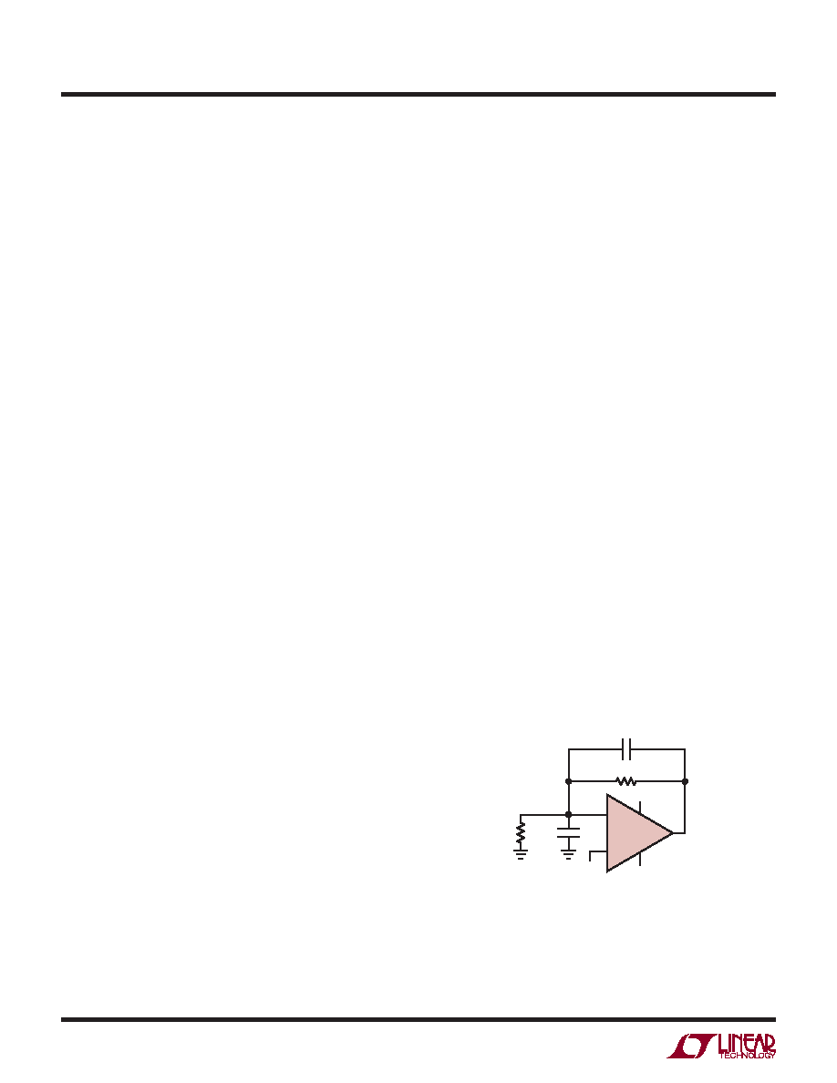
Feedback Components
Care must be taken to ensure that the pole formed by the
feedback resistors and the parasitic capacitance at the
inverting input does not degrade stability. For example, in
a gain of +2 configuration with gain and feedback resis-
tors of 10k, a poorly designed circuit board layout with
parasitic capacitance of 5pF (part +PC board) at the ampli-
fier’s inverting input will cause the amplifier to oscillate
due to a pole formed at 3.2MHz. An additional capacitor
of 5pF across the feedback resistor as shown in Figure 2
will eliminate any ringing or oscillation.
Shutdown
The single and dual versions have SHDN pins that can
shut down the amplifier to less than 7A supply current.
The SHDN pin voltage needs to be within 0.6V of V– for
the amplifier to shut down. During shutdown, the output
will be in high output resistance state, which is suitable
for multiplexer applications. When left floating, the SHDN
pin is internally pulled up to the positive supply and the
amplifier remains enabled.
10k
5pF
CPAR
VOUT
VIN
625567 F02
+
–
LTC6255
Figure 2.
ApplicAtions inForMAtion
相关PDF资料 |
PDF描述 |
|---|---|
| LTC6410IUD-6#PBF | IC AMP DIFF IF 16-QFN |
| LTC6412CUF#TRPBF | IC VGA ANLG-CNTRL 31DB 24-QFN |
| LTC6416IDDB#TRPBF | IC DIFF 16BIT BUFFER 10-DFN |
| LTC6800HDD#TRPBF | IC OP AMP INSTR R-R I/O 8-DFN |
| LTC6910-2HTS8#TRPBF | IC PGA DIGITAL R-R I/O TSOT23-8 |
相关代理商/技术参数 |
参数描述 |
|---|---|
| LTC6256IKC-TRPBF | 制造商:LINER 制造商全称:Linear Technology 功能描述:6.5MHz, 65μA Power Efficient Rail-to-Rail I/O Op Amps |
| LTC6256IMS#PBF | 功能描述:IC OPAMP DUAL 6.5MHZ 10-MSOP RoHS:是 类别:集成电路 (IC) >> Linear - Amplifiers - Instrumentation 系列:- 标准包装:50 系列:- 放大器类型:通用 电路数:2 输出类型:满摆幅 转换速率:1.8 V/µs 增益带宽积:6.5MHz -3db带宽:4.5MHz 电流 - 输入偏压:5nA 电压 - 输入偏移:100µV 电流 - 电源:65µA 电流 - 输出 / 通道:35mA 电压 - 电源,单路/双路(±):1.8 V ~ 5.25 V,±0.9 V ~ 2.625 V 工作温度:-40°C ~ 85°C 安装类型:表面贴装 封装/外壳:10-TFSOP,10-MSOP(0.118",3.00mm 宽) 供应商设备封装:10-MSOP 包装:管件 |
| LTC6256IMS#TRPBF | 功能描述:IC OPAMP DUAL 6.5MHZ 10-MSOP RoHS:是 类别:集成电路 (IC) >> Linear - Amplifiers - Instrumentation 系列:- 标准包装:50 系列:LinCMOS™ 放大器类型:通用 电路数:4 输出类型:- 转换速率:0.05 V/µs 增益带宽积:110kHz -3db带宽:- 电流 - 输入偏压:0.7pA 电压 - 输入偏移:210µV 电流 - 电源:57µA 电流 - 输出 / 通道:30mA 电压 - 电源,单路/双路(±):3 V ~ 16 V,±1.5 V ~ 8 V 工作温度:-40°C ~ 85°C 安装类型:表面贴装 封装/外壳:14-SOIC(0.154",3.90mm 宽) 供应商设备封装:14-SOIC 包装:管件 产品目录页面:865 (CN2011-ZH PDF) 其它名称:296-1834296-1834-5 |
| LTC6256IMS8#PBF | 功能描述:IC OPAMP DUAL 6.5MHZ 8-MSOP RoHS:是 类别:集成电路 (IC) >> Linear - Amplifiers - Instrumentation 系列:- 标准包装:50 系列:- 放大器类型:通用 电路数:2 输出类型:满摆幅 转换速率:1.8 V/µs 增益带宽积:6.5MHz -3db带宽:4.5MHz 电流 - 输入偏压:5nA 电压 - 输入偏移:100µV 电流 - 电源:65µA 电流 - 输出 / 通道:35mA 电压 - 电源,单路/双路(±):1.8 V ~ 5.25 V,±0.9 V ~ 2.625 V 工作温度:-40°C ~ 85°C 安装类型:表面贴装 封装/外壳:10-TFSOP,10-MSOP(0.118",3.00mm 宽) 供应商设备封装:10-MSOP 包装:管件 |
| LTC6256IMS8#TRPBF | 功能描述:IC OPAMP DUAL 6.5MHZ 8-MSOP RoHS:是 类别:集成电路 (IC) >> Linear - Amplifiers - Instrumentation 系列:- 标准包装:50 系列:- 放大器类型:通用 电路数:2 输出类型:满摆幅 转换速率:1.8 V/µs 增益带宽积:6.5MHz -3db带宽:4.5MHz 电流 - 输入偏压:5nA 电压 - 输入偏移:100µV 电流 - 电源:65µA 电流 - 输出 / 通道:35mA 电压 - 电源,单路/双路(±):1.8 V ~ 5.25 V,±0.9 V ~ 2.625 V 工作温度:-40°C ~ 85°C 安装类型:表面贴装 封装/外壳:10-TFSOP,10-MSOP(0.118",3.00mm 宽) 供应商设备封装:10-MSOP 包装:管件 |
发布紧急采购,3分钟左右您将得到回复。