参数资料
| 型号: | LTC6360IDD#PBF |
| 厂商: | Linear Technology |
| 文件页数: | 3/24页 |
| 文件大小: | 0K |
| 描述: | IC ADC DRIVER TRUE ZERO 8DFN |
| 标准包装: | 121 |
| 类型: | ADC 驱动器 |
| 应用: | 数据采集 |
| 安装类型: | 表面贴装 |
| 封装/外壳: | 8-WFDFN 裸露焊盘 |
| 供应商设备封装: | 8-DFN(3x3) |
| 包装: | 管件 |
LTC6360
11
6360f
operaTion
The LTC6360 is a low noise amplifier suitable for driving
single-endedhighperformancesuccessiveapproximation
register (SAR) ADCs. The LTC6360 uses a single ampli-
fier with negative charge pump topology as shown in the
Block Diagram.
The output can swing from –0.48V to 4.91V. The ampli-
fier is designed to drive a series 10Ω resistor and 330pF
capacitor filter network to ground, although larger load
capacitances can be driven.
An on-chip low noise charge pump generates a small
negative voltage (typically –0.6V) at the CPO pin. This
negative voltage is normally connected to the amplifier’s
output stage via the CPI pin, allowing the output to swing
to true zero on a single 5V supply. Compared to typical
rail-to-rail output amplifiers that can only swing to within
a few hundred millivolts of ground, the LTC6360 provides
improved linearity and increased functionality for applica-
tions that benefit from a true zero output swing.
The LTC6360 features a low noise amplifier that can
support a signal-to-noise ratio of 110dB over a 3MHz
noise bandwidth.
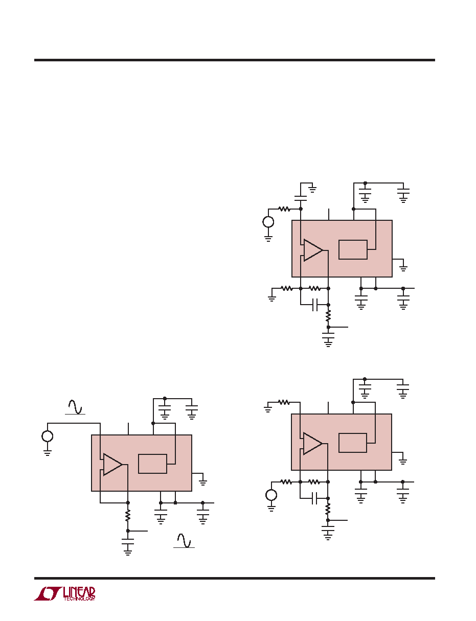
Basic Connections
Shown in Figure 2 is a typical application for the LTC6360
as a unity gain driver. The amplifier’s two inputs (+IN and
–IN) can accommodate a voltage range of 0V to 4.25V on
a single 5V rail. This provides a simple interface for 5V
ADCs with a 4.096V full-scale range.
Noninverting gain (shown in Figure 3) and inverting gain
(shown in Figure 4) configurations are also possible. For
best DC precision, RS should be made equal to the paral-
lel combination of RF and RG. RS can be bypassed with a
capacitor to reduce its noise contribution.
Figure 2. Unity Gain Driver.
Figure 3. Noninverting Gain Configuration.
Figure 4. Inverting Gain Configuration
5V
VIN
0V TO 4V
10
0.1F
5V
6360 F02
CPO
VDD
GND
LTC6360
OUT
–IN
VCC
VOUT
CPI
SHDN
+IN
–
+
CHARGE
PUMP
0.1F
10F
330pF
+–
4V
0V
VIN
4V
0V
1F
5V
VIN
RS
0.1F
5V
6360 F03
CPO
VDD
GND
LTC6360
OUT
–IN
VCC
VOUT
RF
CF
RG
CPI
SHDN
+IN
–
+
CHARGE
PUMP
0.1F
10F
+–
1F
RFILT
CFILT
CS
5V
RS
0.1F
5V
6360 F04
CPO
VDD
GND
LTC6360
OUT
–IN
VCC
VOUT
RF
RG
VIN
CPI
SHDN
+IN
–
+
CHARGE
PUMP
0.1F
10F
+–
CF
1F
RFILT
CFILT
相关PDF资料 |
PDF描述 |
|---|---|
| VE-B5H-MX-S | CONVERTER MOD DC/DC 52V 75W |
| LTC6360IMS8E#PBF | IC ADC DRIVER TRUE ZERO 8MSOP |
| VE-B5D-MX-S | CONVERTER MOD DC/DC 85V 75W |
| AD8138AARMZ-RL | IC ADC DRIVER DIFF 8MSOP |
| VE-B5B-MX-S | CONVERTER MOD DC/DC 95V 75W |
相关代理商/技术参数 |
参数描述 |
|---|---|
| LTC6360IMS8E#PBF | 功能描述:IC ADC DRIVER TRUE ZERO 8MSOP RoHS:是 类别:集成电路 (IC) >> 线性 - 放大器 - 专用 系列:- 产品培训模块:Lead (SnPb) Finish for COTS Obsolescence Mitigation Program 标准包装:60 系列:- 类型:可变增益放大器 应用:CATV 安装类型:表面贴装 封装/外壳:20-WQFN 裸露焊盘 供应商设备封装:20-TQFN-EP(5x5) 包装:托盘 |
| LTC6360IMS8E#TRPBF | 功能描述:IC ADC DRIVER TRUE ZERO 8MSOP RoHS:是 类别:集成电路 (IC) >> 线性 - 放大器 - 专用 系列:- 产品培训模块:Lead (SnPb) Finish for COTS Obsolescence Mitigation Program 标准包装:60 系列:- 类型:可变增益放大器 应用:CATV 安装类型:表面贴装 封装/外壳:20-WQFN 裸露焊盘 供应商设备封装:20-TQFN-EP(5x5) 包装:托盘 |
| LTC6362 | 制造商:LINER 制造商全称:Linear Technology 功能描述:Precision, Low Power Rail-to-Rail Input/Output |
| LTC6362CDD#PBF | 功能描述:IC OPAMP DIFFERENTIAL R-R 8DFN RoHS:是 类别:集成电路 (IC) >> Linear - Amplifiers - Instrumentation 系列:- 标准包装:1,000 系列:- 放大器类型:电压反馈 电路数:4 输出类型:满摆幅 转换速率:33 V/µs 增益带宽积:20MHz -3db带宽:30MHz 电流 - 输入偏压:2nA 电压 - 输入偏移:3000µV 电流 - 电源:2.5mA 电流 - 输出 / 通道:30mA 电压 - 电源,单路/双路(±):4.5 V ~ 16.5 V,±2.25 V ~ 8.25 V 工作温度:-40°C ~ 85°C 安装类型:表面贴装 封装/外壳:14-SOIC(0.154",3.90mm 宽) 供应商设备封装:14-SOIC 包装:带卷 (TR) |
| LTC6362CDD#TRPBF | 功能描述:IC OPAMP DIFFERENTIAL R-R 8DFN RoHS:是 类别:集成电路 (IC) >> Linear - Amplifiers - Instrumentation 系列:- 标准包装:1,000 系列:- 放大器类型:电压反馈 电路数:4 输出类型:满摆幅 转换速率:33 V/µs 增益带宽积:20MHz -3db带宽:30MHz 电流 - 输入偏压:2nA 电压 - 输入偏移:3000µV 电流 - 电源:2.5mA 电流 - 输出 / 通道:30mA 电压 - 电源,单路/双路(±):4.5 V ~ 16.5 V,±2.25 V ~ 8.25 V 工作温度:-40°C ~ 85°C 安装类型:表面贴装 封装/外壳:14-SOIC(0.154",3.90mm 宽) 供应商设备封装:14-SOIC 包装:带卷 (TR) |
发布紧急采购,3分钟左右您将得到回复。