参数资料
| 型号: | LTC6400IUD-26#TRPBF |
| 厂商: | Linear Technology |
| 文件页数: | 12/16页 |
| 文件大小: | 0K |
| 描述: | IC ADC DRIVER DIFF 16-QFN |
| 标准包装: | 2,500 |
| 类型: | ADC 驱动器 |
| 应用: | 数据采集 |
| 安装类型: | 表面贴装 |
| 封装/外壳: | 16-WFQFN 裸露焊盘 |
| 供应商设备封装: | 16-QFN-EP(3x3) |
| 包装: | 带卷 (TR) |
LTC6400-26
5
640026fa
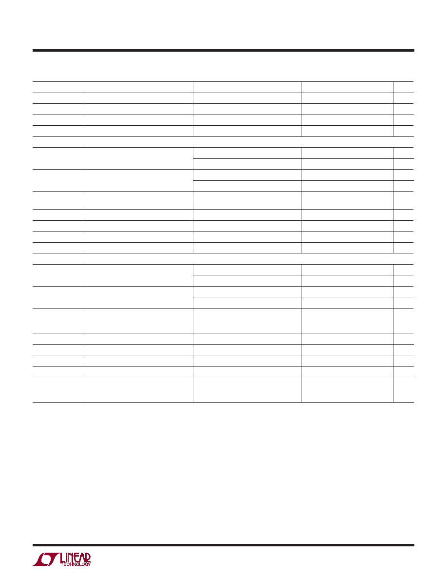
SYMBOL
PARAMETER
CONDITIONS
MIN
TYP
MAX
UNITS
P1dB,140M
1dB Compression Point
RL = 375Ω (Notes 5, 7)
18.7
dBm
NF140M
Noise Figure
RL = 375Ω (Note 5)
6.6
dB
eN,140M
Input Referred Voltage Noise Density
Includes Resistors (Short Inputs)
1.4
nV/√Hz
eON,140M
Output Referred Voltage Noise Density
Includes Resistors (Short Inputs)
28
nV/√Hz
240MHz Input Signal
HD2,240M/
HD3,240M
Second/Third Order Harmonic Distortion
2VP-P,OUT, RL = 200Ω
–70/–59
dBc
2VP-P,OUT, No RL
–75/–71
dBc
IMD3,240M
Third Order Intermodulation
(f1 = 239.5MHz f2 = 240.5MHz)
2VP-P,OUT Composite, RL = 200Ω
–70
dBc
2VP-P,OUT Composite, No RL
–76
dBc
OIP3,240M
Third Order Output Intercept Point
(f1 = 239.5MHz f2 = 240.5MHz)
2VP-P,OUT Composite, No RL (Note 7)
42
dBm
P1dB,240M
1dB Compression Point
RL = 375Ω (Notes 5, 7)
18.1
dBm
NF240M
Noise Figure
RL = 375Ω (Note 5)
6.9
dB
eN,240M
Input Referred Voltage Noise Density
Includes Resistors (Short Inputs)
1.4
nV/√Hz
eON,240M
Output Referred Voltage Noise Density
Includes Resistors (Short Inputs)
28
nV/√Hz
300MHz Input Signal
HD2,300M/
HD3,300M
Second/Third Order Harmonic Distortion
2VP-P,OUT, RL = 200Ω
–66/–54
dBc
2VP-P,OUT, No RL
–76/–62
dBc
IMD3,300M
Third Order Intermodulation
(f1 = 299.5MHz f2 = 300.5MHz)
2VP-P,OUT Composite, RL = 200Ω
–66
dBc
2VP-P,OUT Composite, No RL
–71
dBc
OIP3,300M
Equivalent Third Order Output Intercept
Point
(f1 = 299.5MHz f2 = 300.5MHz)
2VP-P,OUT Composite, No RL (Note 7)
39.5
dBm
P1dB,300M
1dB Compression Point
RL = 375Ω (Notes 5, 7)
17.7
dBm
NF300M
Noise Figure
RL = 375Ω (Note 5)
7.6
dB
eN,300M
Input Referred Voltage Noise Density
Includes Resistors (Short Inputs)
1.5
nV/√Hz
eON,300M
Output Referred Voltage Noise Density
Includes Resistors (Short Inputs)
30
nV/√Hz
IMD3,280M/320M
Third Order Intermodulation
(f1 = 280MHz f2 = 320MHz) Measured at
360MHz
2VP-P,OUT Composite, RL = 375Ω
–68
–62
dBc
AC ELECTRICAL CHARACTERISTICS Specications are at T
A = 25°C. V
+ = 3V, V– = 0V, VOCM = 1.25V,
ENABLE = 0V, No RL unless otherwise noted.
Note 1: Stresses beyond those listed under Absolute Maximum Ratings
may cause permanent damage to the device. Exposure to any Absolute
Maximum Rating condition for extended periods may affect device
reliability and lifetime.
Note 2: Input pins (+IN, –IN) are protected by steering diodes to either
supply. If the inputs go beyond either supply rail, the input current should
be limited to less than 10mA.
Note 3: The LTC6400C is guaranteed functional over the operating
temperature range of –40°C to 85°C.
Note 4: The LTC6400C is guaranteed to meet specied performance from
0°C to 70°C. It is designed, characterized and expected to meet specied
performance from –40°C to 85°C but is not tested or QA sampled at these
temperatures. The LTC6400I is guaranteed to meet specied performance
from –40°C to 85°C.
Note 5: Input and output baluns used. See Test Circuit A.
Note 6: Measured using Test Circuit B. RL = 87.5Ω per output.
Note 7: Since the LTC6400-26 is a feedback amplier with low output
impedance, a resistive load is not required when driving an AD converter.
Therefore, typical output power is very small. In order to compare the
LTC6400-26 with ampliers that require 50
Ω output load, the LTC6400-26
output voltage swing driving a given RL is converted to OIP3 and P1dB as
if it were driving a 50
Ω load. Using this modied convention, 2VP-P is by
denition equal to 10dBm, regardless of actual RL.
相关PDF资料 |
PDF描述 |
|---|---|
| LTC6400IUD-8#TRPBF | IC ADC DRIVER DIFF 2.2GHZ 16QFN |
| LTC6401CUD-14#PBF | IC ADC DRIVER DIFF 16-QFN |
| LTC6401CUD-20#PBF | IC ADC DRIVER DIFF 16-QFN |
| LTC6401CUD-26#PBF | IC ADC DRIVER DIFF 16-QFN |
| LTC6401IUD-8#TRPBF | IC ADC DRIVER DIFF 16-QFN |
相关代理商/技术参数 |
参数描述 |
|---|---|
| LTC6400IUD-8 | 制造商:LINER 制造商全称:Linear Technology 功能描述:2.4GHz Low Noise, Low Distortion Differential ADC Driver for 300MHz IF |
| LTC6400IUD-8#PBF | 功能描述:IC ADC DRIVER DIFF 2.2GHZ 16QFN RoHS:是 类别:集成电路 (IC) >> 线性 - 放大器 - 专用 系列:- 产品培训模块:Lead (SnPb) Finish for COTS Obsolescence Mitigation Program 标准包装:60 系列:- 类型:可变增益放大器 应用:CATV 安装类型:表面贴装 封装/外壳:20-WQFN 裸露焊盘 供应商设备封装:20-TQFN-EP(5x5) 包装:托盘 |
| LTC6400IUD-8#TR | 制造商:Linear Technology 功能描述:DIFF-AMPLIFIER, 2.2GHZ, QFN-16, No. of Amplifiers:1, Input Offset Voltage:5mV, Gain dB Max:8dB, Bandwidth:2.2GHz, Amplifier Case Style:QFN, No. of Pins:16, Supply Voltage Range:2.85V to 3.5V, Slew Rate:3810V/s, Supply Current:85mA , RoHS Compliant: No |
| LTC6400IUD-8#TRPBF | 功能描述:IC ADC DRIVER DIFF 2.2GHZ 16QFN RoHS:是 类别:集成电路 (IC) >> 线性 - 放大器 - 专用 系列:- 产品培训模块:Lead (SnPb) Finish for COTS Obsolescence Mitigation Program 标准包装:60 系列:- 类型:可变增益放大器 应用:CATV 安装类型:表面贴装 封装/外壳:20-WQFN 裸露焊盘 供应商设备封装:20-TQFN-EP(5x5) 包装:托盘 |
| LTC6400IUD-8-PBF | 制造商:LINER 制造商全称:Linear Technology 功能描述:2.2GHz Low Noise, Low Distortion Differential ADC Driver for DC-300MHz |
发布紧急采购,3分钟左右您将得到回复。